Intel Joins Musk's $25B Terafab as Foundry Partner
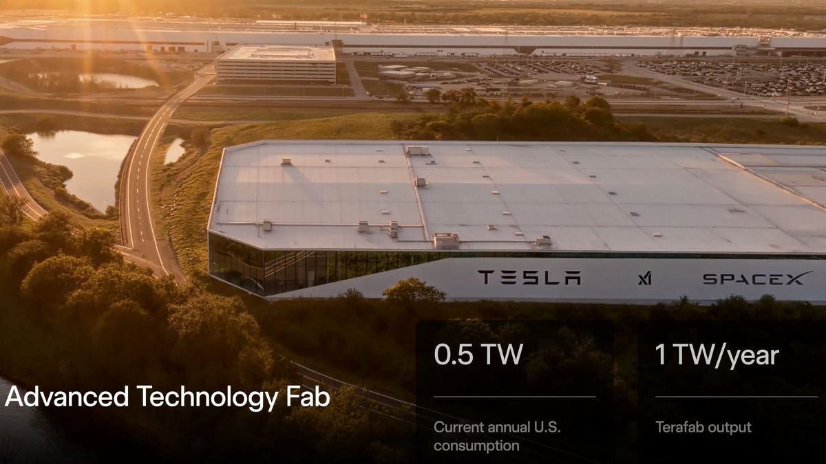
Intel will use its 18A process node to manufacture chips for the Tesla-SpaceX-xAI joint venture targeting 1 terawatt of AI compute annually - and claims $2B in CHIPS Act subsidies in the process.
Intel has been looking for an anchor customer to validate its foundry pivot since Lip-Bu Tan took the CEO chair in March 2025. On April 7, it found one - though the order is large enough to make even optimists pause.
The company announced it'll join Terafab as the primary foundry and manufacturing partner, contributing its 18A process node, the most advanced semiconductor process currently in commercial production in the United States, to a $25 billion joint venture between Tesla, SpaceX, and xAI. The announcement sent Intel shares up 4% on the day to $52.91, with the gain extending past 10% by the close of April 8 as markets absorbed the scope of the commitment.
TL;DR
- Intel becomes primary foundry partner for Terafab, the $25B chip joint venture between Tesla, SpaceX, and xAI, announced April 7
- Intel's 18A process node (1.8nm-class) will manufacture Tesla AI5 and AI6 chips for humanoid robots and AVs, plus radiation-hardened processors for SpaceX's orbital data centers
- Intel Foundry, which previously generated $307M in external customer revenue, gains its first anchor client since Tan's restructuring began
- The deal qualifies Intel for roughly $2B in CHIPS Act federal subsidies; Terafab itself targets 1 terawatt of AI compute capacity annually by full buildout
The Financial Picture
The numbers are hard to contextualise because they're large in ways that strain credibility. Terafab targets 100 to 200 billion custom AI and memory chips per year at full capacity, starting from 100,000 wafer starts per month and scaling toward one million. The facility at Giga Texas North Campus in Austin would span roughly 100 million square feet - Elon Musk's own estimate - which is around ten times the size of the main Giga Texas building, itself nearly a mile long.
Intel's 18A node reached commercially viable yields of 65% in early April, a milestone the company has been working toward for two years. The timing of the Terafab announcement with that yield confirmation wasn't accidental.
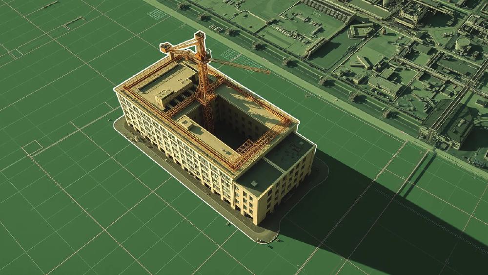
 Tesla's Terafab North Campus announced in March 2026. Construction is already visible on the east side of Giga Texas.
Source: electrek.co
Tesla's Terafab North Campus announced in March 2026. Construction is already visible on the east side of Giga Texas.
Source: electrek.co
| Metric | Before Terafab | With Terafab |
|---|---|---|
| Intel Foundry external revenue | $307M annually | $25B JV anchor client |
| 18A process yield (early April 2026) | 65% commercially viable | Full production ramp |
| Intel stock (April 7-8 move) | ~$48 pre-announcement | $52.91 (+4%), then +10% two-day |
| CHIPS Act subsidy eligibility | Uncertain | ~$2B direct federal subsidies |
Who Benefits
Intel: The Anchor Customer It Has Chased for Two Years
Intel's foundry business is the central bet of Tan's turnaround plan. The problem has been circular: without a credible anchor client, it couldn't prove the technology at scale; without proof at scale, it couldn't attract anchor clients. The $307M in external Foundry revenue Intel reported previously didn't make a difference against TSMC's tens of billions.
Terafab changes the calculus. Producing chips for Tesla's AI5 and AI6 silicon - the processors that'll drive Optimus humanoid robots and the Cybercab autonomous vehicle fleet - at scale means Intel Foundry will be processing meaningful wafer volumes within 12 to 18 months. That volume gives Intel data, yield improvements, and credibility it can show to the next prospective customer, including, as the company has publicly signalled, Apple and Qualcomm.
The CHIPS Act angle matters too. The $2B in federal subsidies attached to Terafab construction offsets some of the capital investment risk at a moment when Intel's balance sheet cannot absorb a high-profile miss.
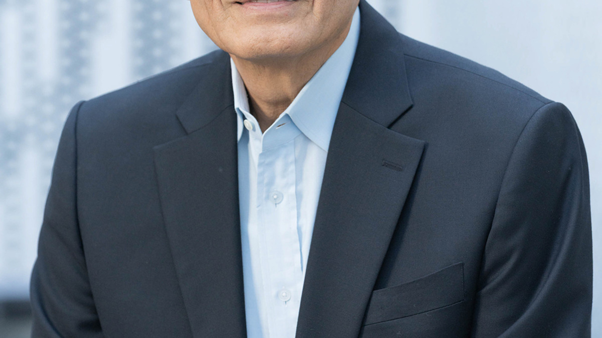 Intel CEO Lip-Bu Tan, appointed March 2025, has restructured the company around external foundry clients under the IDM 2.0 strategy.
Source: newsroom.intel.com
Intel CEO Lip-Bu Tan, appointed March 2025, has restructured the company around external foundry clients under the IDM 2.0 strategy.
Source: newsroom.intel.com
Musk's Empire: Vertical Control Over the Compute Stack
For Tesla, SpaceX, and xAI - which SpaceX absorbed in February in a deal valuing the combined entity at $1.25 trillion - Terafab represents the logical endpoint of Musk's vertical integration strategy. The company already designs its own AI silicon (FSD, Dojo, and the AI5/AI6 chips under development). Owning the fab means owning the full stack from model training to chip tape-out to production hardware.
The split in production priorities is clarifying: 80% of Terafab's output is earmarked for SpaceX's orbital AI data centers - radiation-hardened chips designed to operate in space aboard the Starlink-based constellation - and 20% for ground applications including Tesla's robotics and automotive lines. This is mainly a space compute play with automotive production as a secondary revenue stream.
Elon Musk first disclosed Terafab at a presentation at Giga Texas on March 21, pitching a facility targeting one terawatt of annual AI compute capacity - roughly 50 times total global AI compute output in 2025.
Who Pays
The Terafab Gamble
The gap between announced ambition and proved capacity is substantial. One terawatt of annual AI compute isn't a production target; it's a vision. The initial ramp - 100,000 wafer starts per month - is meaningful but nowhere near the scale the headline implies. Getting from there to one million wafer starts requires capital, time, and a sustained relationship with a customer base that is, for now, almost completely internal to the Musk portfolio.
Intel's 65% yield on 18A is commercially viable but not exceptional. TSMC's comparable node runs higher. For chips going into humanoid robots and orbital satellites, where defect tolerance is low and reliability requirements are severe, yield improvements will need to continue before Terafab can ship at the volumes it projects.
There's also an ongoing debate about whether Intel's chip architecture choices are well-suited to agentic AI workloads - a question that won't be resolved by a new fab agreement alone.
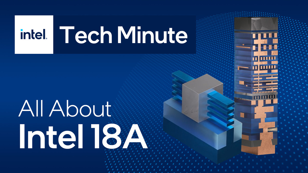 Intel's 18A process node combines RibbonFET gate-all-around transistors with PowerVia backside power delivery.
Source: newsroom.intel.com
Intel's 18A process node combines RibbonFET gate-all-around transistors with PowerVia backside power delivery.
Source: newsroom.intel.com
The Public Bill
The $2B in CHIPS Act subsidies that Terafab qualifies for is federal money directed at a joint venture whose primary customer, by volume, is a private satellite network. The CHIPS Act was designed to reshore semiconductor manufacturing for national security reasons. Whether chips heading to SpaceX's orbital data centers satisfy that intent is a question Washington will eventually have to answer.
Musk's relationship with the federal government is, to put it gently, complicated. He simultaneously runs a government cost-cutting project and is now a beneficiary of one of its largest industrial subsidy programs.
Intel has spent two years arguing that its foundry business can compete with TSMC. Terafab gives it the chance to prove that claim - at a scale where failure isn't recoverable.
Sources:
- Intel signs on to Elon Musk's Terafab chips project - TechCrunch
- Intel joins Musk's Terafab as foundry partner in $25B chip megaproject - The Next Web
- Tesla files site plans for massive Giga Texas expansion including 'ecological paradise' - Electrek
- The 18A Renaissance: Intel and Musk's 'Terafab' Project Redefines Global AI Compute - MarketMinute
- Intel 18A Process Technology Simply Explained - Intel Newsroom

