
Google's Frozen v2 Chip Bakes Gemini Into Silicon
Google is reportedly building a chip line separate from its TPUs that hardwires parts of Gemini directly into silicon, promising up to 10x efficiency as a capacity crunch forces Cloud to turn away customers.
 6 min read
Source: pexels.com
Google is designing a chip that doesn't just run Gemini faster. It's trying to make Gemini part of the chip itself.
TL;DR
- The Information reports Google is building "Frozen v2," a chip line separate from its TPU roadmap that hardwires elements of Gemini's architecture directly into silicon
- The approach could deliver 6-10x more efficiency than Google's newest custom chips, measured in tokens served per watt
- Targeted for 2028, the project is a response to a capacity crunch severe enough that Google Cloud has been turning away outside customers
- Alphabet shares rose about 3% on the report; Google declined to confirm or deny specifics, pointing instead to its "full stack" hardware-software strategy
What Google Is Actually Building
According to The Information's reporting, Google engineers are still finalizing the design, including exactly how much of Gemini's architecture gets committed to hardware. But the direction is set: a chip that treats a specific model, not a general-purpose accelerator target, as the thing being optimized for.
Baking a Model Into Hardware
Every AI chip on the market today, including Google's own TPUs, is built to run any transformer-shaped workload reasonably well. Frozen v2 flips that. By embedding parts of Gemini's architecture directly into the silicon, Google strips out the general-purpose flexibility that normally costs power and die space, cutting the calculations and data movement needed to answer a query. It's the chip equivalent of swapping a Swiss Army knife for the one blade you actually use, sharpened far past what a folding knife allows.
A Parallel Line, Not a TPU Replacement
Frozen v2 isn't the eighth generation of Google's Tensor Processing Unit line. It runs alongside it. Google's TPUs, most recently the seventh-generation Ironwood chip that shipped in late 2025 with 192GB of HBM3E memory and 4,614 FP8 TFLOPS per chip, remain Google's general-purpose AI silicon, sold as a cloud service to Anthropic, Meta, and other customers. Frozen chips, by contrast, appear to be an internal-use project built to make Google's own Gemini inference cheaper, not a product Google plans to rent out.
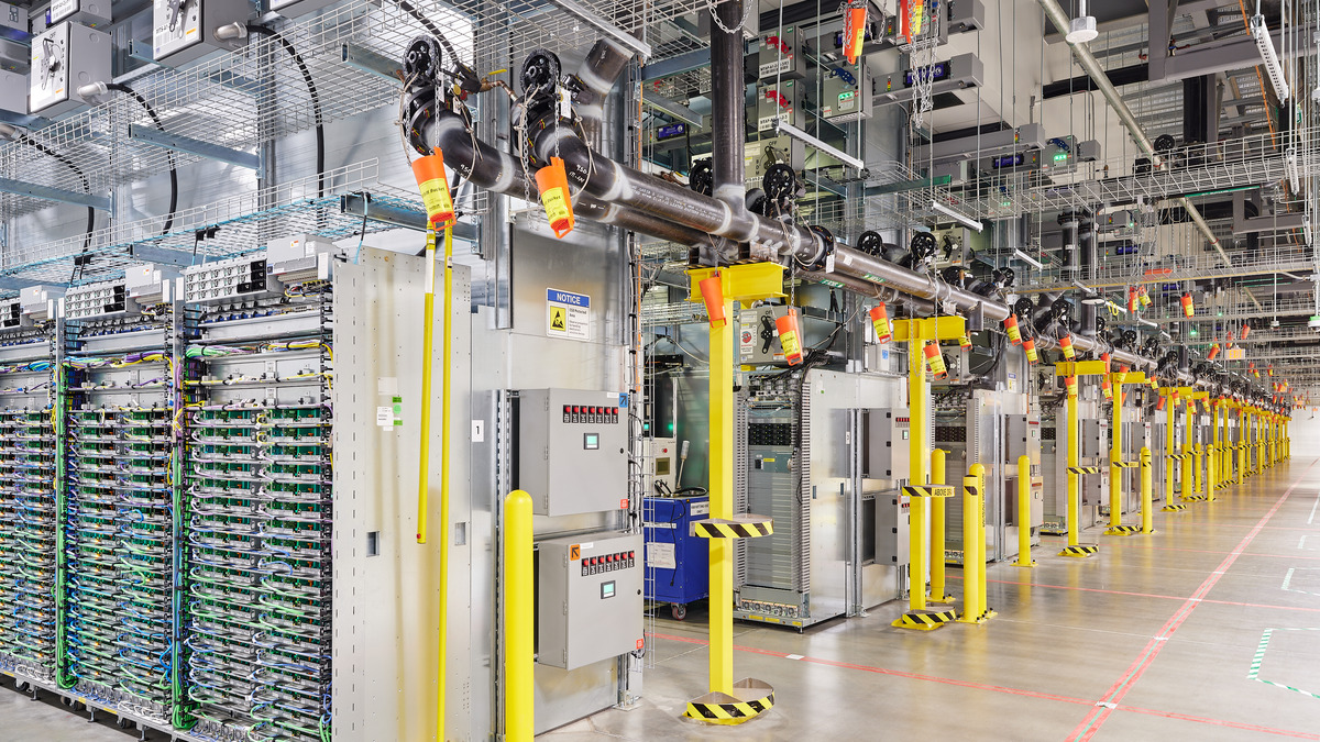 Server aisles inside Google's New Albany, Ohio data center. The capacity crunch driving Frozen v2 has reportedly led Google Cloud to decline deals with outside customers.
Source: datacenters.google
Server aisles inside Google's New Albany, Ohio data center. The capacity crunch driving Frozen v2 has reportedly led Google Cloud to decline deals with outside customers.
Source: datacenters.google
Why Now: The Capacity Math
Google isn't building Frozen v2 for speed's own sake. It's building it because Gemini's compute demand has outrun Google's ability to provision hardware, a problem serious enough that Google Cloud has reportedly been passing on outside contracts to keep capacity for Gemini itself. The rough logic behind Frozen v2 looks something like this:
Baseline: N chips running Gemini at current TPU efficiency
Frozen v2 claim: same N chips deliver 6-10x tokens/watt
Result: same power budget, 6-10x more Gemini inference,
        OR same inference volume at roughly 1/6 to 1/10 the power draw
That math matters more than a typical hardware refresh because Google isn't choosing between "faster" and "not faster." It's choosing between building more data centers, which takes years and gigawatts of power procurement, and squeezing more Gemini capacity out of the data centers it already has. Anthropic's $200 billion Google Cloud compute commitment, signed earlier this year, only tightened that same capacity pool further.
Where This Sits Next to Everything Else Google Runs
| Chip line | Approach | Efficiency claim | Timeline | Status |
|---|---|---|---|---|
| Ironwood (TPU v7) | General-purpose inference accelerator | ~4x prior TPU generation | Shipping since late 2025 | In production, sold via Google Cloud |
| Frozen v2 | Gemini-specific, model baked into silicon | 6-10x tokens/watt vs newest TPUs | Targeted 2028 | In design, unconfirmed by Google |
| Nvidia GPU (industry baseline) | General-purpose accelerator, any model | N/A (Google's comparison point) | Shipping | Google's primary external dependency |
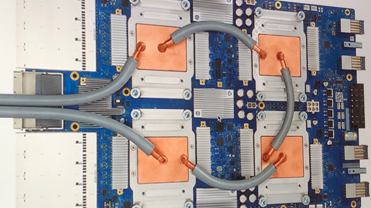 One of Google's earlier liquid-cooled TPU pod boards. Frozen v2 would run as a separate, Gemini-specific line alongside chips like this rather than replacing them.
Source: commons.wikimedia.org
One of Google's earlier liquid-cooled TPU pod boards. Frozen v2 would run as a separate, Gemini-specific line alongside chips like this rather than replacing them.
Source: commons.wikimedia.org
The Nvidia Angle
Google has spent a decade building its own silicon to avoid full dependence on Nvidia, and Frozen v2 extends that logic further than any hyperscaler has gone public with. Meta is chasing the same goal with its Iris chip, moving into production this September on a 2nm process to cut its own Nvidia and AMD spend. Neither company is abandoning Nvidia GPUs outright, but both are betting that model-specific or workload-specific silicon is where the next efficiency gains have to come from, since general-purpose accelerator performance is no longer improving fast enough to keep pace with model growth on its own.
Where It Falls Short
None of this is confirmed by Google. The company's only on-record response, from a Google Cloud spokesperson, was that it's "constantly researching and experimenting with new innovations" through a "full stack approach" of co-designed hardware and software - confirming the general strategy without confirming the chip, its name, or its numbers.
The timeline is also doing a lot of work here. 2028 is far enough out that Gemini's architecture, the thing this chip is supposedly being built around, will likely change more than once before the silicon ships. Baking a model into hardware creates an obsolescence risk a general-purpose TPU doesn't carry: if Gemini's next architecture shift is significant enough, Frozen v2 could end up optimized for a model Google has already moved past. Google's own engineers are reportedly still undecided on how much of the model to commit to hardware for exactly this reason.
There's also a gap between a reported internal project and a shipped product. Custom AI silicon has a track record of slipping, and the industry's closest comparison, Meta's Iris chip, is only now entering production years after MTIA was first announced. A six-to-tenfold efficiency claim, sourced to anonymous engineers two years before tape-out, is a target, not a benchmark result.
What the report does confirm, even without Google's sign-off, is how tight the compute math has gotten inside the companies building frontier models. When a company with Google's chip design history and TPU fleet is reportedly building a second, narrower chip line just to keep up with its own model's demand, that's a clearer signal about AI's power and capacity constraints than any efficiency percentage on a slide.
Sources:
- Google is working on a new AI chip designed to make Gemini more efficient - TechCrunch
- Google plans new chip to run Gemini models more efficiently, the Information reports - Yahoo Finance
- Alphabet stock pops on report it's developing a more efficient AI chip - CNBC
- Ironwood: The first Google TPU for the age of inference - Google Blog
- Google's decade-long bet on custom chips is turning into company's secret weapon in AI race - CNBC

