Ayar Labs Raises $500M to Wire AI Chips With Light
Ayar Labs closes a $500M Series E backed by Nvidia, AMD, and Sequoia to mass-produce co-packaged optical interconnects that replace copper in AI data centers.

Ayar Labs has closed a $500 million Series E funding round, valuing the startup at $3.75 billion and pushing its total outside funding to $870 million. The round was led by Neuberger Berman, with Nvidia and AMD participating as strategic investors with MediaTek, Qatar Investment Authority, Alchip Technologies, ARK Invest, Insight Partners, and Sequoia Capital.
The company builds co-packaged optics - silicon photonic chips that replace copper interconnects inside AI server clusters with light-based links. That sounds like a narrow engineering problem. The investors apparently think it's the next major bottleneck in artificial intelligence infrastructure.
TL;DR
- Ayar Labs closes $500M Series E at a $3.75 billion valuation
- Led by Neuberger Berman; Nvidia, AMD, Sequoia, and QIA among investors
- Total funding now $870M across all rounds
- Technology replaces copper chip-to-chip links with optical fiber
- Claims 4x to 20x more throughput per watt vs copper
- Capital goes toward volume production and a new Taiwan office
Why Copper Is Losing the Race
The problem Ayar is selling against is real and getting worse. As AI training and inference clusters scale, the electrical signals traveling through copper traces between chips degrade. Higher currents increase signal noise, energy losses mount, and the distances that data can travel without degradation shrink. This isn't a software problem. It is physics.
Ayar's TeraPHY chiplets transmit data as light rather than electrons. The company's next-generation design, with eight chiplets per package, supports more than 200 terabits per second of aggregate bandwidth. For context, Nvidia's Rubin GPU architecture supports 28.8 terabits per second per package on its copper interconnects. The optical figure is roughly seven times higher.
The energy math is similarly stark. Ayar claims its optical interconnects deliver between four and twenty times more compute throughput per watt compared to conventional copper connections. In a world where data centers are struggling to secure power and cooling capacity, that efficiency gap matters.
Nvidia itself has been moving money into photonics. As we covered when Nvidia committed $4 billion to photonics partnerships with Lumentum and Coherent, the company has been building a position in optical interconnect technology for over a year. Backing Ayar directly - as a strategic investor in this round - is the next step in that same thesis.
The TeraPHY Architecture
Ayar's system uses two components. The SuperNova chip produces the laser light source. The TeraPHY chiplet encodes data onto that light and can process up to eight terabits of traffic per second in its current generation. The chiplets use the UCIe standard, which allows them to integrate directly with GPUs and other processors as co-packaged components rather than external modules.
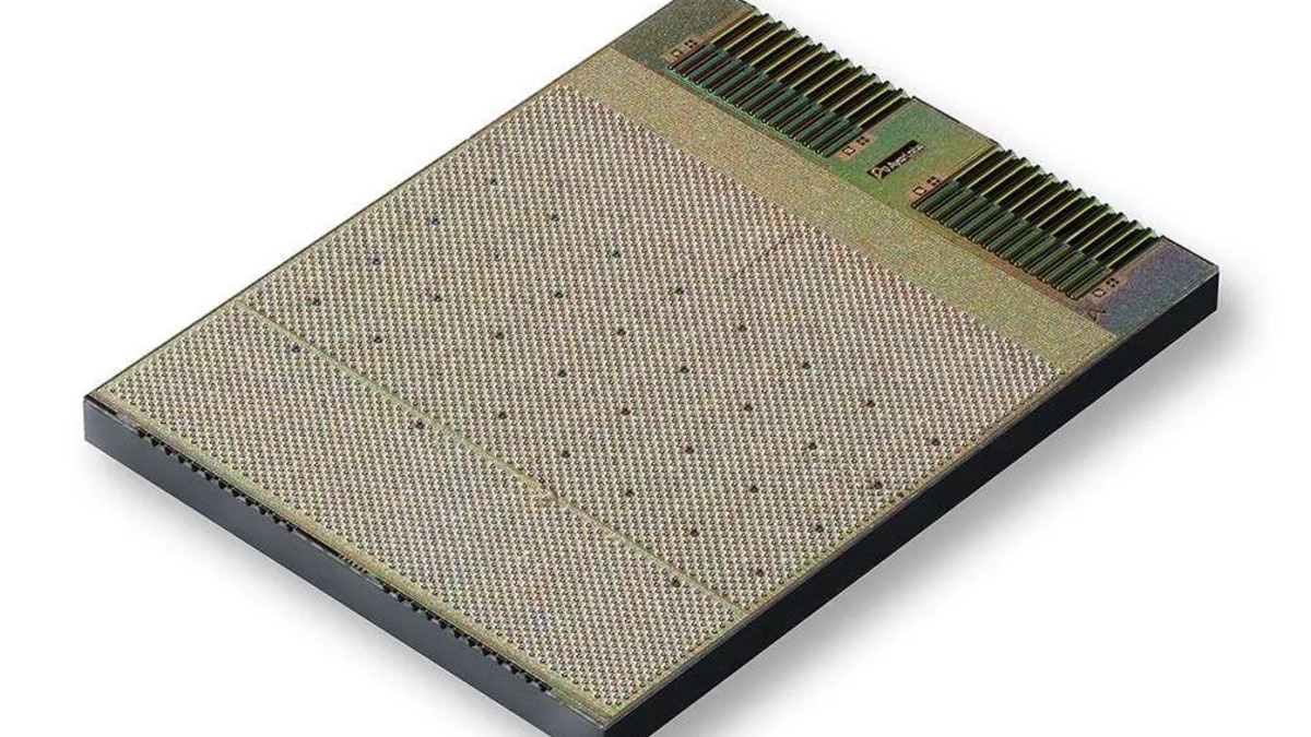 Ayar Labs' TeraPHY 8 Tbps UCIe optical I/O chiplet, which co-packages directly with GPUs and other processors. Photo: Ayar Labs.
The company has also built reference designs with Alchip and Global Unichip Corp, two of the largest chip design service firms in Taiwan, which explains the new Hsinchu office. Volume production requires proximity to the advanced packaging ecosystem.
Who Benefits
Hyperscalers and cloud providers are the most direct beneficiaries. For companies running tens of thousands of GPUs in tightly coupled training clusters, the latency and bandwidth ceiling imposed by copper links is a genuine constraint on model scale. Meta's multibillion-dollar GPU buildout with Nvidia is exactly the kind of deployment where interconnect bandwidth becomes a first-order constraint. Optical interconnects remove that ceiling, at least for chip-to-chip communication within a rack or between adjacent racks.
Nvidia and AMD benefit in a different way. By backing Ayar as a strategic investor, both companies make sure co-packaged optics technology is available and compatible with their own GPU architectures before competitors lock in an alternative standard. Pat Gelsinger, the former Intel CEO who sits on Ayar's board, knows from experience what happens when a company cedes the interconnect layer to a competitor.
Ayar's existing investors - Sequoia, ARK Invest, Insight Partners - benefit from the signal sent by having the two dominant GPU makers participate in the same round. That's not a typical outcome for a hardware startup.
Competitive Landscape
| Company | Approach | Backing | Status |
|---|---|---|---|
| Ayar Labs | Co-packaged optics (CPO) | Nvidia, AMD, Sequoia | Volume production ramp |
| Intel | Optical Compute Interconnect (OCI) | In-house | Demo stage |
| Lumentum | Pluggable optics + photonics | Nvidia investment | Production |
| Coherent | Silicon photonics transceivers | Nvidia investment | Production |
Ayar's co-packaged approach is more tightly integrated than pluggable optics solutions, which improves latency and power efficiency but also makes it harder to swap out. That's a larger bet on a single architecture.
Who Pays
Ayar Labs carries the execution risk. The company has spent fifteen years developing its core technology, according to CEO Mark Wade. The challenge now is manufacturing at scale. Co-packaged optics require advanced packaging processes - the TeraPHY chiplets need to be integrated directly with processors during chip production, not added later. That demands tight coordination with foundries and packaging partners.
Customers will pay a premium over copper for the first generation of products. The unit economics of photonics at scale are still being proven. The 4x to 20x efficiency claim is a wide range, which suggests real-world performance depends heavily on workload type and deployment configuration.
 Dense GPU clusters like these are where copper interconnects hit their limits - and where optical fiber now promises to take over.
The broader AI infrastructure ecosystem absorbs the transition cost if co-packaged optics becomes the dominant standard. Existing server designs, rack configurations, and supply chains are built around copper. Replacing them is an industry-wide capital event, not just a product decision for one vendor.
The rational question is whether Ayar has timed this correctly. Co-packaged optics has been described as the next interconnect revolution for the better part of a decade. What has changed is that AI training clusters have grown large enough that copper's physical limits are now a visible constraint rather than a theoretical one. With Nvidia and AMD both in the cap table and volume production imminent, the technology is closer to deployment than the hype cycle suggests - though whether Ayar captures the value or becomes infrastructure for someone else's margin is still an open question.
Sources:
- Ayar Labs Closes $500M Series E, Accelerates Volume Production of Co-Packaged Optics - TechFundingNews
- Co-packaged optics startup Ayar Labs raises $500M round backed by Nvidia, AMD - SiliconANGLE
- Ayar Labs raises $500M to mass-produce CPO chiplets - The Register
- Nvidia-backed Ayar Labs raises $500M to speed AI chips with light-based interconnects - TechStartups
