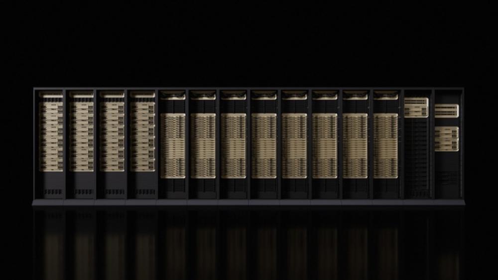
NVIDIA Rubin R200 - Next-Gen AI Superchip
Complete specs, benchmarks, and analysis of the NVIDIA Rubin R200 GPU - the post-Blackwell flagship with 288GB HBM4, 22 TB/s bandwidth, and 50 PFLOPS FP4.
TL;DR
- 336 billion transistors across two TSMC N3P compute dies - 1.6x more than the B200's 208 billion
- 288GB HBM4 at 22 TB/s bandwidth - nearly triple Blackwell's 8 TB/s - removes the memory wall for trillion-parameter models
- 50 PFLOPS NVFP4 sparse inference and 35 PFLOPS NVFP4 training per GPU - a 5x and 3.5x leap over Blackwell respectively
- NVIDIA claims 10x lower cost per inference token and 4x fewer GPUs needed to train MoE models versus Blackwell
- Shipping H2 2026 through AWS, Azure, GCP, OCI, CoreWeave, Lambda, and Nebius
Overview
The NVIDIA Rubin R200 is the first GPU built on NVIDIA's Rubin architecture, and it represents the company's most aggressive generational leap in datacenter AI compute. Announced at CES 2026 and entering full production for H2 2026 shipment, the R200 delivers 50 PFLOPS of sparse NVFP4 inference performance per GPU - 5x the B200's 10 PFLOPS. That's not a typo. NVIDIA is claiming a full 5x inference uplift in a single generation.
The architecture marks several firsts. The R200 is NVIDIA's first GPU on TSMC's 3nm-class N3P process node, its first to use HBM4 memory (288GB at 22 TB/s), and its first to deploy NVLink 6 at 3.6 TB/s bidirectional per GPU. The chip packs 336 billion transistors across two near-reticle compute dies connected via NVIDIA's SoIC 3D vertical stacking, continuing the multi-chiplet approach proven by Blackwell's dual-die design but pushing it to a new level of integration.
Where Blackwell changed the cost curve for inference, Rubin aims to break it. NVIDIA claims the Vera Rubin NVL72 system - pairing 72 R200 GPUs with 36 Vera CPUs - can deliver 10x lower cost per inference token compared to the equivalent Blackwell configuration. For MoE model training, NVIDIA says it takes one-quarter the GPUs. If those numbers hold under independent benchmarks, Rubin doesn't just obsolete Blackwell - it redefines what's economically viable to train and serve.
Key Specifications
| Specification | Details |
|---|---|
| Manufacturer | NVIDIA |
| Architecture | Rubin (R200, dual compute die) |
| Process Node | TSMC N3P (compute), N5B (I/O dies) |
| Transistors | 336 billion |
| Streaming Multiprocessors | 224 |
| Tensor Cores | 5th generation |
| GPU Memory | 288 GB HBM4 (8 x 36GB stacks) |
| Memory Bandwidth | 22,000 GB/s (22 TB/s) |
| NVFP4 Inference (sparse) | 50 PFLOPS |
| NVFP4 Training | 35 PFLOPS |
| FP8/FP6 Training | 17.5 PFLOPS |
| FP16 / BF16 | 4 PFLOPS |
| TF32 | 2 PFLOPS |
| FP32 | 130 TFLOPS (vector), 400 TFLOPS (matrix) |
| FP64 | 33 TFLOPS (vector), 200 TFLOPS (matrix) |
| INT8 | 250 TOPS |
| NVLink 6 | 3.6 TB/s bidirectional (36 links) |
| NVLink-C2C (CPU-GPU) | 1.8 TB/s coherent |
| PCIe | Gen 6 |
| Packaging | SoIC 3D stacking + CoWoS |
| TDP | ~1,200W estimated per GPU module |
| Form Factor | Vera Rubin Superchip (2 GPUs + 1 Vera CPU) |
| Release Date | H2 2026 |
The R200's 336 billion transistors represent a 1.6x increase over the B200's 208 billion and a 4.2x increase over the H100's 80 billion. NVIDIA reaches this through two near-reticle compute dies fabricated on TSMC N3P, connected via SoIC 3D vertical stacking - a denser interconnect approach than Blackwell's NV-HBI. The I/O chiplets use the more cost-effective N5B node, a practical multi-process design that tunes silicon costs.
The 224 SMs house NVIDIA's fifth-generation Tensor Cores with expanded Special Function Units (SFUs) optimized for attention, activation, and sparse compute. Softmax acceleration doubles compared to Blackwell, with 32 FP32 and 64 FP16 SFU EX2 operations per clock per SM - a targeted optimization for transformer inference where softmax is a recurring bottleneck.
Performance Benchmarks
| Metric | H100 SXM | B200 | Rubin R200 | R200 vs B200 |
|---|---|---|---|---|
| NVFP4 Inference (sparse) | N/A | 18,000 TFLOPS | 50 PFLOPS | ~2.8x |
| FP8 Training (dense) | 1,979 TFLOPS | 4,500 TFLOPS | 17,500 TFLOPS | 3.9x |
| FP16/BF16 | 990 TFLOPS | 2,250 TFLOPS | 4,000 TFLOPS | 1.8x |
| TF32 | 990 TFLOPS | 2,250 TFLOPS | 2,000 TFLOPS | ~0.9x |
| Memory Capacity | 80 GB HBM3 | 192 GB HBM3e | 288 GB HBM4 | 1.5x |
| Memory Bandwidth | 3,350 GB/s | 8,000 GB/s | 22,000 GB/s | 2.75x |
| NVLink Bandwidth | 900 GB/s | 1,800 GB/s | 3,600 GB/s | 2x |
| Transistors | 80B | 208B | 336B | 1.6x |
| Process Node | TSMC 4N | TSMC 4NP | TSMC N3P | 1 node |
The headline numbers demand context. The 5x inference claim compares Rubin's sparse NVFP4 to Blackwell's NVFP4. The real-world gain depends on how well models quantize to FP4 and whether workloads are compute-bound or memory-bound. For memory-bandwidth-limited inference - which is the common case for autoregressive LLM decoding - the 2.75x bandwidth improvement (22 TB/s vs 8 TB/s) is arguably the more impactful spec. That bandwidth increase means Rubin can feed tokens through larger models without starving the Tensor Cores.
The training story is equally compelling. At 17.5 PFLOPS FP8, the R200 delivers nearly 4x the B200's FP8 training throughput. Combined with the 2x NVLink bandwidth improvement (reducing all-reduce communication overhead) and the 2.75x memory bandwidth (reducing data loading stalls), the compound effect on distributed training throughput should be major. NVIDIA's claim that Rubin requires 4x fewer GPUs to train MoE models appears plausible given these numbers, though independent validation is needed.
Key Capabilities
HBM4 Memory at 22 TB/s. The R200 is the first datacenter GPU to ship with HBM4, which doubles the interface width compared to HBM3e. NVIDIA co-engineered new memory controllers that deliver nearly 3x the bandwidth of Blackwell (22 TB/s vs 8 TB/s). The 288GB capacity at this bandwidth is significant for two reasons: it enables serving larger models on fewer GPUs, and it removes the memory bandwidth bottleneck that limits autoregressive decoding throughput on current hardware. A 70B model at FP4 (~35GB) leaves over 250GB for KV-cache - enough for massive batch sizes or very long context windows.
NVLink 6 at 3.6 TB/s. Each R200 GPU supports 36 NVLink 6 connections providing 3.6 TB/s of bidirectional bandwidth - double Blackwell's NVLink 5. In the Vera Rubin NVL72 configuration, 72 GPUs form a unified all-to-all NVLink domain with 260 TB/s of aggregate scale-up bandwidth. The NVLink-C2C interface provides 1.8 TB/s of coherent bandwidth between the Vera CPU and Rubin GPUs, enabling unified memory access across CPU and GPU address spaces.
Vera CPU Co-Design. The Rubin platform pairs each pair of R200 GPUs with one Vera CPU - a custom 88-core Arm v9.2 processor with 176 threads (using Spatial Multithreading), 1.5TB LPDDR5X memory, and 1.2 TB/s memory bandwidth. The Vera CPU offers 2.4x higher memory bandwidth and 3x greater memory capacity than Grace, providing substantial CPU-side compute for data preprocessing, orchestration, and agentic AI workloads that interleave CPU and GPU computation.
Pricing and Availability
NVIDIA has not disclosed per-GPU pricing for the R200. For reference, the previous-generation GB200 NVL72 rack was reported at roughly $3 million. The Vera Rubin NVL72 is expected to carry a premium given the die size and HBM4 cost increases, though the 5x inference performance improvement should deliver a lower cost per token.
| Detail | Information |
|---|---|
| GPU Price (individual) | Not disclosed |
| NVL72 Rack (estimated) | $3M-$5M (industry estimates) |
| Cooling cost per NVL144 | ~$55,710 (liquid cooling system) |
| Cloud availability | H2 2026 |
| Cloud providers | AWS, Azure, GCP, OCI, CoreWeave, Lambda, Nebius, Nscale |
Cloud provider deployments are confirmed from AWS, Google Cloud, Microsoft Azure, and Oracle Cloud, with NVIDIA Cloud Partners CoreWeave, Lambda, Nebius, and Nscale. Volume shipments begin H2 2026, though meaningful non-hyperscaler availability may extend into early 2027. OpenAI has announced a strategic partnership to deploy the first gigawatt of NVIDIA systems on the Vera Rubin platform.
The cooling economics are standout: liquid cooling for a single Vera Rubin NVL144 rack is estimated at $55,710 - a 17% increase over the GB300 NVL72's $49,860. At the system level, cooling costs are a small fraction of total hardware cost but highlight the infrastructure complexity of rolling out Rubin at scale.
Strengths
- 50 PFLOPS NVFP4 sparse inference per GPU - 5x Blackwell, enabling dramatically lower cost per token
- 288GB HBM4 at 22 TB/s - nearly 3x the bandwidth of the B200, removing the memory wall for inference
- 336 billion transistors on TSMC N3P with SoIC 3D stacking - the densest datacenter GPU ever built
- NVLink 6 at 3.6 TB/s doubles multi-GPU interconnect bandwidth for better distributed training scaling
- Vera CPU with 88 Olympus cores and 1.5TB LPDDR5X provides sizable CPU-side compute for agentic AI
- NVLink-C2C at 1.8 TB/s enables coherent CPU-GPU memory access with minimal latency
- PCIe Gen 6 connectivity for future-proof I/O bandwidth
- 10x lower cost per inference token claimed vs Blackwell - if validated, a transformative improvement
Weaknesses
- Not yet shipping - H2 2026 availability with potential supply constraints extending into 2027
- No official per-GPU pricing; rack-level costs expected to be $3M-$5M based on industry estimates
- Estimated ~1,200W+ per GPU module requires liquid cooling - no air-cooled option
- HBM4 is a first-generation memory technology with potential yield and cost premiums
- NVIDIA's 5x and 10x claims are marketing projections pending independent benchmark validation
- Rubin Ultra (with HBM4e) already on the roadmap for 2027, creating potential buyer hesitation
- Software stack optimizations for Rubin-specific features (FP4, new SFU operations) will take time to mature
- 600kW+ rack power for Kyber-class deployments requires purpose-built datacenter infrastructure
Related Coverage
- NVIDIA B200 - Blackwell Flagship GPU - The current-gen GPU that Rubin succeeds
- NVIDIA GB200 NVL72 - Rack-Scale Blackwell - Blackwell's rack system, similar to the Vera Rubin NVL72
- NVIDIA GB300 NVL72 - Blackwell Ultra - Blackwell Ultra with 288GB HBM3e
- NVIDIA H100 SXM - The AI Training Benchmark - Two generations back but still widely deployed
- NVIDIA H200 - Inference-Optimized Hopper - Memory-optimized Hopper variant
Sources
- NVIDIA Vera Rubin NVL72 Product Page
- NVIDIA Newsroom - Rubin Platform Announcement
- Inside the NVIDIA Rubin Platform - NVIDIA Technical Blog
- Vera Rubin Platform Obsoletes Current AI Iron - The Next Platform
- Tom's Hardware - Vera Rubin NVL72 at CES
- NVIDIA Rubin Architecture - Wikipedia
- Rubin R200 Specs - Glenn Klockwood
- Tom's Hardware - Vera Rubin Power Boost to 2300W
- Vera Rubin NVL144 Cooling Costs - TechRadar
- NVIDIA Rubin Platform Overview
