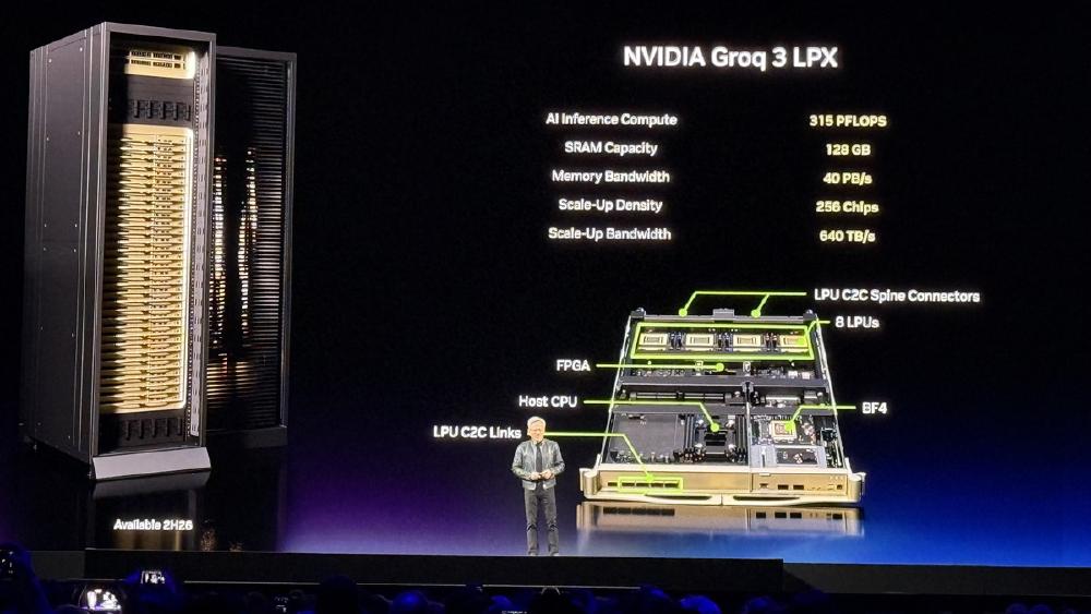
NVIDIA Groq 3 LPU - SRAM-Based Inference Engine
The NVIDIA Groq 3 LPU is a pure-SRAM inference chip delivering 150 TB/s memory bandwidth and 1.2 PFLOPS FP8 per chip, designed to pair with Vera Rubin GPUs for trillion-parameter model serving.
TL;DR
- Pure-SRAM architecture: 500MB on-chip SRAM per chip, 150 TB/s bandwidth - 7x faster than Vera Rubin GPU memory
- 1.2 PFLOPS FP8 per chip; full LPX rack packs 256 chips for 315 PFLOPS and 40 PB/s aggregate
- Pairs with Vera Rubin NVL72: GPU handles prefill, LPU handles decode - 35x more throughput per megawatt for trillion-parameter models
- Ships Q3 2026 on Samsung 4nm; NVIDIA acquired Groq technology for $20B in December 2025
Overview
The NVIDIA Groq 3 LPU is the outcome of the biggest acqui-hire in AI hardware history. NVIDIA licensed Groq's Language Processing Unit technology for $20 billion in December 2025, integrating it with the Vera Rubin platform announced at CES. Jensen Huang unveiled the Groq 3 at GTC 2026 in March as the first chip in the Rubin ecosystem that isn't a GPU - a purpose-built decoder designed for one job: creating output tokens at the lowest possible cost and latency.
The fundamental design choice is radical. Where every GPU from NVIDIA's H100 to AMD's MI300X pairs compute cores with external HBM memory, the Groq 3 removes HBM completely. Each chip holds 500MB of SRAM directly on the die, connected at 150 TB/s. That is seven times faster than the Vera Rubin GPU's 22 TB/s HBM bandwidth. The tradeoff is capacity: 500MB per chip versus 288GB of HBM on a Rubin GPU. For the decode phase of inference, which repeatedly reads the same weight matrices at low arithmetic intensity, this turns out to be exactly the right trade.
NVIDIA didn't design the Groq 3 as a standalone product. It's a platform component. In the intended deployment, Rubin GPUs handle prefill - processing the input prompt with high compute intensity - and hand off to Groq 3 LPUs for decode, where the model produces each output token sequentially. This disaggregated serving architecture keeps both halves of the cluster doing what they're good at, rather than using expensive GPU compute for a memory-bound task.
Key Specifications
| Specification | Details |
|---|---|
| Manufacturer | NVIDIA (via Groq technology) |
| Product Family | Groq LPU (3rd generation) |
| Chip Type | Language Processing Unit (LPU) |
| Process Node | Samsung 4nm |
| On-Chip SRAM | 500MB per chip |
| Memory Bandwidth | 150 TB/s per chip |
| FP8 Performance | 1.2 PFLOPS per chip |
| Training Support | None |
| Architecture | Deterministic data-flow; linear SRAM pipeline |
| Rack Config (LPX) | 256 LPUs across 32 trays (8 LPUs per tray) |
| LPX Aggregate SRAM | 128GB |
| LPX Aggregate Bandwidth | 40 PB/s |
| LPX Aggregate FP8 | 315 PFLOPS |
| Scale-Up Bandwidth | 640 TB/s (per LPX rack) |
| TDP | Not disclosed |
| Release Date | Q3 2026 |
| Pricing | Not disclosed |
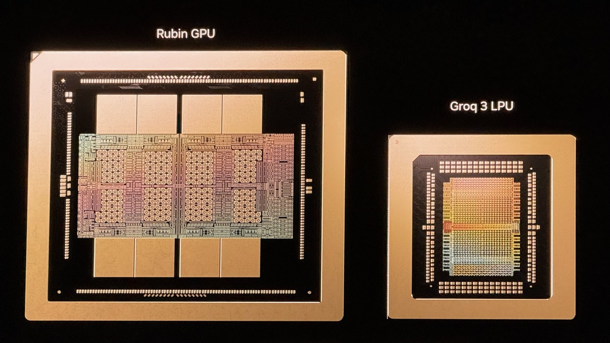 The Groq 3 LPU's 500MB SRAM die sits with a Vera Rubin GPU - the architectural difference is the entire product strategy.
Source: Tom's Hardware / NVIDIA
The Groq 3 LPU's 500MB SRAM die sits with a Vera Rubin GPU - the architectural difference is the entire product strategy.
Source: Tom's Hardware / NVIDIA
Performance Benchmarks
Comparing the Groq 3 LPU to GPUs on the same metrics isn't quite right - they're not competing for the same workload. The relevant comparison is the full Vera Rubin NVL72 + Groq 3 LPX system versus an equivalently sized Blackwell NVL72 cluster.
| Metric | Groq 3 LPU | H100 SXM5 | B200 SXM6 | Vera Rubin GPU |
|---|---|---|---|---|
| Memory bandwidth | 150 TB/s | 3.35 TB/s | 8.0 TB/s | 22 TB/s |
| FP8 compute (per chip) | 1.2 PFLOPS | 3.96 PFLOPS | 9 PFLOPS | ~50 PFLOPS |
| On-chip memory | 500MB SRAM | - | - | 288GB HBM |
| Training support | No | Yes | Yes | Yes |
| Deterministic latency | Yes | No | No | No |
| Tok/s (70B FP8, single chip) | ~500-750 | ~100 | ~200 | ~250 |
| Joules per token (70B) | 1-3 | 10-30 | ~8 | ~5 |
The efficiency numbers are the headline story. At 1-3 joules per token on 70B models versus 10-30 joules for comparable GPU setups, the Groq 3 consumes roughly one-tenth the energy per output token. NVIDIA claims the combined NVL72 + LPX system delivers 35x more inference throughput per megawatt than a Blackwell NVL72 alone for trillion-parameter workloads.
That figure warrants scrutiny. The 35x claim applies specifically to trillion-parameter models with continuous batching, where the decode phase leads total compute time. For smaller models or more balanced prefill-heavy workloads - such as RAG pipelines with long inputs and short outputs - the advantage shrinks or disappears. The Groq 3 LPU is optimized for a specific traffic pattern, not for general inference.
Key Capabilities
The Groq 3's core architectural differentiator is determinism. Every inference request on every chip runs in exactly the same number of clock cycles, regardless of batch size or sequence length. This matters for serving infrastructure: you can predict latency exactly, set SLA guarantees without padding, and avoid the latency spikes that affect GPU-based serving under variable load. The original Groq architecture from startup days built this property into the chip design, and it's preserved in the third generation.
The LPX rack format pairs 256 Groq 3 chips into a system with chip-to-chip copper connections and 640 TB/s of scale-up bandwidth. Multiple LPX racks can be federated to act as a single inference engine for very large models. NVIDIA recommends a 3:1 GPU-to-LPU ratio for mixed inference fleets - roughly 25% of compute capacity in LPU form.
Deployment requires a disaggregated serving architecture, which adds operational complexity. The Rubin GPU cluster and the Groq LPX rack need to hand off between prefill and decode phases, managed by NVIDIA's inference software stack. Teams running vLLM or TensorRT-LLM today will need to adopt the disaggregated serving pattern. This is non-trivial to set up, and not all workloads benefit from the separation.
Integration with the Rubin Platform
The Groq 3 LPU isn't sold as a standalone device for typical customers. It's part of the Vera Rubin NVL144 and GB300 NVL72 platform, where NVIDIA positions the combination as essential for competitive trillion-parameter inference economics. The target price point NVIDIA has stated is $45 per million tokens at system scale - a meaningful improvement over current H100-based inference pricing.
For contrast, the original Groq LPU used a 14nm GlobalFoundries process with 230MB SRAM and ~750 TFLOPS FP8. The Groq 3 is a sizable generational upgrade: Samsung 4nm, 500MB SRAM, 1.2 PFLOPS FP8, and 150 TB/s bandwidth versus the first generation's 80 TB/s.
Pricing and Availability
Groq 3 LPU pricing hasn't been disclosed. NVIDIA plans cloud availability through AWS, Google Cloud, Microsoft Azure, and Oracle Cloud in Q3 2026, with the Groq 3 LPX rack available as an add-on to Vera Rubin NVL72 deployments. On-premises pricing for enterprises isn't yet announced.
The $45/million token target is a system-level claim that requires the full NVL72 + LPX combination. Current H100 inference pricing runs $0.16-$0.33 per million tokens depending on provider, and B200-based inference is expected near $0.10-0.15. The Groq 3 combination targets a further reduction, though the 35x throughput improvement doesn't map linearly to a proportional cost reduction since it's measured per megawatt, not per dollar of hardware.
Strengths
- 150 TB/s SRAM bandwidth per chip - 7x faster than Vera Rubin GPU for decode-phase inference
- Deterministic latency with no variance across batch sizes or sequence lengths
- 35x more inference throughput per megawatt than Blackwell NVL72 alone (trillion-parameter, NVIDIA claim)
- Tight hardware-software integration with NVIDIA's full inference stack
- In volume production Q3 2026 on proven Samsung 4nm
Weaknesses
- No training, fine-tuning, or multi-purpose compute
- Requires disaggregated serving architecture (prefill GPU + decode LPU) - increased ops complexity
- 500MB SRAM per chip limits the model classes it can serve without multi-chip federation
- Performance advantage degrades for prefill-heavy workloads (RAG, long-context QA)
- All published benchmarks are vendor-supplied; independent validation pending
Related Coverage
- Original Groq LPU - the startup's first-generation SRAM chip that NVIDIA built upon
- NVIDIA Vera Rubin NVL144 - the primary platform the Groq 3 LPU pairs with
- NVIDIA GB300 NVL72 - the Blackwell system the Rubin + LPX combination outperforms on inference
- GTC 2026 coverage at awesomeagents.ai
Sources
- IEEE Spectrum: NVIDIA Groq 3 LPU
- Tom's Hardware: Groq 3 LPU and LPX racks join Rubin platform at GTC
- The Register: NVIDIA slaps Groq into new LPX racks
- The Register: A closer look at NVIDIA's LPX rack systems
- The Decoder: With Groq 3 LPX, NVIDIA adds dedicated inference hardware
- Spheron: NVIDIA Groq 3 LPU explained
- NVIDIA GTC 2026 - Vera Rubin Platform
✓ Last verified April 15, 2026
