NVIDIA B200 - Blackwell Flagship GPU
Complete specs, benchmarks, and analysis of the NVIDIA B200 - the Blackwell-architecture flagship GPU with 192GB HBM3e, 8 TB/s bandwidth, and up to 9,000 TFLOPS FP8.
TL;DR
- 192GB HBM3e with 8,000 GB/s (8 TB/s) bandwidth - 2.4x the memory and bandwidth of the H100 in a single GPU
- 9,000 TFLOPS dense FP8 and up to 18,000 TFLOPS sparse FP4 - a 2.3x compute leap over Hopper on transformer workloads
- Revolutionary dual-die design with 208 billion transistors on TSMC 4NP - 2.6x more transistors than the H100
- Fifth-generation NVLink at 1,800 GB/s doubles the interconnect bandwidth for multi-GPU scaling
- 1,000W TDP requires liquid cooling for most deployments - a significant datacenter infrastructure investment
Overview
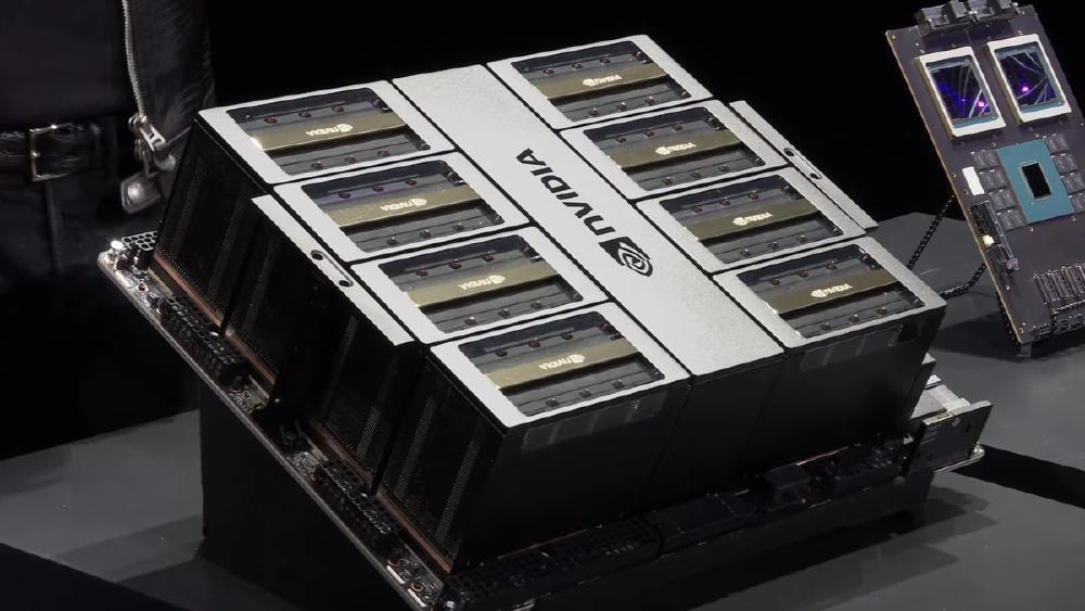
The NVIDIA B200 is the flagship GPU of the Blackwell generation, and it represents the largest single-generation performance leap in NVIDIA datacenter GPU history. Shipping from early 2025, the B200 delivers 9,000 TFLOPS of dense FP8 compute - 2.3x more than the H100's 3,958 TFLOPS with sparsity. It packs 192GB of HBM3e at 8,000 GB/s, 2.4x the H100's capacity and bandwidth. And it does this on a revolutionary dual-die architecture that stitches two GB202 dies together with a 10 TB/s NV-HBI interconnect, packing 208 billion transistors into what functions as a single monolithic GPU.
The Blackwell architecture introduces fifth-generation Tensor Cores with native FP4 support, enabling up to 18,000 TFLOPS of sparse FP4 throughput per GPU. FP4 is particularly relevant for inference workloads where quantization to 4-bit precision is increasingly viable with modern quantization techniques like GPTQ and AWQ. At FP4, the B200 delivers roughly 5x the inference throughput of the H100 - a number that fundamentally changes the economics of deploying large language models at scale.
But the B200 is not a free upgrade. It draws 1,000W - 43% more than the H100's 700W - and most deployments require liquid cooling. The DGX B200 system with eight GPUs consumes over 14.3kW, roughly doubling the power footprint of a DGX H100. For hyperscalers building new capacity, this is a datacenter design parameter, not a showstopper. For organizations retrofitting existing air-cooled facilities, the B200's thermal requirements may push them toward the H200 or force expensive infrastructure upgrades before they can deploy Blackwell.
Key Specifications
| Specification | Details |
|---|---|
| Manufacturer | NVIDIA |
| Architecture | Blackwell (GB202, dual-die) |
| Process Node | TSMC 4NP |
| Transistors | 208 billion (2x GB202 dies) |
| Die Size | ~750 mm² per die (dual-die package) |
| CUDA Cores | 18,432 |
| Tensor Cores | 576 (5th generation) |
| Streaming Multiprocessors | 148 |
| GPU Memory | 192 GB HBM3e |
| Memory Bandwidth | 8,000 GB/s (8 TB/s) |
| Memory Bus Width | 8,192-bit |
| L2 Cache | 96 MB (4 partitions) |
| FP64 Performance | 45 TFLOPS (90 TFLOPS with sparsity) |
| FP32 Performance | 90 TFLOPS (180 TFLOPS with sparsity) |
| TF32 Performance | 2,250 TFLOPS (4,500 TFLOPS with sparsity) |
| FP16 / BF16 Performance | 2,250 TFLOPS (4,500 TFLOPS with sparsity) |
| FP8 Performance | 4,500 TFLOPS (9,000 TFLOPS with sparsity) |
| FP4 Performance | 9,000 TFLOPS (18,000 TFLOPS with sparsity) |
| Transformer Engine | 2nd generation (FP8/FP4 dynamic) |
| NVLink | 5th generation, 1,800 GB/s |
| PCIe | Gen 5.0 x16 |
| Multi-Instance GPU | Yes |
| Inter-Die Bandwidth | 10 TB/s (NV-HBI) |
| TDP | 1,000W |
| Form Factor | SXM, HGX |
| Cooling | Liquid cooling recommended |
| Release Date | Q1 2025 |
The B200's 208 billion transistors represent a 2.6x increase over the H100's 80 billion. This was made possible by the dual-die design - two GB202 dies, each fabricated near the reticle limit of TSMC's 4NP process, connected by NVIDIA's proprietary NV-HBI (High-Bandwidth Interface) at 10 TB/s. The dual-die approach is an engineering landmark: it breaks through the reticle limit that has constrained GPU die sizes for over a decade, enabling transistor counts that would be physically impossible on a single die.
Each GB202 die contains approximately 104 billion transistors and houses half of the GPU's compute and memory controller resources. The NV-HBI interconnect runs at 10 TB/s - higher than the 8 TB/s external memory bandwidth - ensuring that the two dies behave as a single unified compute domain with no visible performance penalty from the die boundary. From a software perspective, the B200 presents as a single monolithic GPU. No special programming is required to exploit both dies.
The 96 MB L2 cache (doubled from the H100's 50 MB, organized into 4 partitions) provides even more on-chip data reuse. For inference workloads where model weights are accessed repeatedly, the larger L2 reduces HBM traffic and improves effective bandwidth. The four L2 partitions (two per die) are connected through the NV-HBI fabric, maintaining a unified cache coherency domain.
Performance Benchmarks
| Metric | A100 80GB | H100 SXM | H200 | B200 |
|---|---|---|---|---|
| FP8 Tensor TFLOPS (dense) | N/A | 1,979 | 1,979 | 4,500 |
| FP8 Tensor TFLOPS (sparse) | N/A | 3,958 | 3,958 | 9,000 |
| FP4 Tensor TFLOPS (sparse) | N/A | N/A | N/A | 18,000 |
| Memory Capacity | 80 GB HBM2e | 80 GB HBM3 | 141 GB HBM3e | 192 GB HBM3e |
| Memory Bandwidth | 2,039 GB/s | 3,350 GB/s | 4,800 GB/s | 8,000 GB/s |
| NVLink Bandwidth | 600 GB/s | 900 GB/s | 900 GB/s | 1,800 GB/s |
| TDP | 400W | 700W | 700W | 1,000W |
| Transistors | 54.2B | 80B | 80B | 208B |
| Process | TSMC 7N | TSMC 4N | TSMC 4N | TSMC 4NP |
The B200 versus H100 comparison is striking across every axis. Dense FP8 compute improves 2.3x (4,500 vs 1,979 TFLOPS). Memory capacity increases 2.4x (192 vs 80 GB). Memory bandwidth increases 2.4x (8,000 vs 3,350 GB/s). NVLink bandwidth doubles (1,800 vs 900 GB/s). NVIDIA claims the B200 delivers up to 4x faster training and 30x faster inference compared to the H100, with the inference number driven primarily by the new FP4 precision and larger memory pool.
Training Performance Analysis
The 4x training speedup claim applies to large transformer models trained with the second-generation Transformer Engine at FP8 precision. The improvement breaks down as follows: 2.3x from raw FP8 compute improvement, an additional ~1.5x from the higher memory bandwidth reducing data starvation, and further gains from the doubled NVLink bandwidth improving multi-GPU scaling efficiency. The product of these improvements lands near 4x for well-optimized distributed training workloads.
In practice, the training speedup varies significantly with model size and training configuration. For a 7B-parameter model on a single GPU, the improvement is closer to 2.5-3x because the NVLink advantage does not apply. For 70B+ models trained across 8 GPUs (where NVLink scaling matters), the improvement approaches 4x. For trillion-parameter models trained across hundreds of GPUs (where the 72-GPU NVLink domain of the GB200 NVL72 provides the biggest advantage), the system-level improvement can exceed 4x.
Inference Performance Analysis
The 30x inference claim deserves context. It applies to specific large-model inference scenarios where the H100 is severely memory-bandwidth-limited and where FP4 quantization can be applied without unacceptable accuracy degradation. On compute-bound training workloads at the same precision, the improvement is closer to 2-3x.
For batch-1 inference on a 70B model, the B200's advantages compound: 2.4x more bandwidth (8 TB/s vs 3.35 TB/s), plus 2x from FP4 quantization reducing the bytes per weight from 2 (FP16) to 0.5 (FP4), plus elimination of multi-GPU sharding (the model fits on one B200 at FP4 but might need 2 H100s at FP16). The combined effect can easily reach 10-15x for this specific scenario. The 30x number likely includes optimizations specific to NVIDIA's TensorRT-LLM inference engine that exploit Blackwell-specific hardware features.
At production batch sizes (32-256), the B200's advantage over the H100 narrows to roughly 3-5x, which is still an enormous generational improvement. The key insight is that FP4 inference on Blackwell is not just faster - it changes the cost curve. A single B200 at FP4 can do the work of 3-5 H100s at FP8, making inference dramatically cheaper per token.
Key Capabilities
Dual-Die Architecture with NV-HBI. The B200 is the first NVIDIA datacenter GPU to use a multi-chip module (MCM) design. Two GB202 dies, each manufactured at the reticle limit of TSMC's 4NP process, are connected via NVIDIA's High-Bandwidth Interface (NV-HBI) at 10 TB/s. This is not a compromise design - the inter-die bandwidth exceeds the memory bandwidth, ensuring that the two dies function as a single unified compute domain. The dual-die approach allowed NVIDIA to pack 208 billion transistors into a single GPU package - 2.6x more than the H100's 80 billion - without being constrained by reticle size limits. It is an engineering achievement that sets the template for future GPU scaling.
The NV-HBI interface uses a novel packaging technology that places the two dies close together on a silicon interposer, minimizing the signal path length and power consumption of the inter-die link. The 10 TB/s bandwidth is bidirectional (5 TB/s in each direction), providing sufficient bandwidth for both dies to share L2 cache data and coordinate Tensor Core operations without bottlenecks. In benchmarks, the performance penalty from the die boundary is immeasurable - the B200 performs identically to a hypothetical monolithic GPU with the same specifications.
Second-Generation Transformer Engine with FP4. The B200 introduces the second-generation Transformer Engine, which extends dynamic precision management to include FP4 alongside FP8 and FP16. The engine automatically selects the optimal precision per layer and per tensor, now with three precision options instead of two. FP4 inference is where the B200's real performance story lives: at 18,000 TFLOPS sparse FP4, the B200 can process inference tokens at roughly 5x the throughput of the H100's best FP8 performance.
The FP4 format is not simply "half of FP8." NVIDIA's implementation uses a block-scaled FP4 with per-channel scaling factors stored in higher precision, which preserves more of the original model's accuracy than naive 4-bit quantization. The second-generation Transformer Engine manages these scaling factors automatically, similar to how the first-generation engine managed FP8 scaling. For production inference deployments where quantization to 4-bit is acceptable - and modern quantization methods make this viable for most language models - FP4 on Blackwell is transformative.
Fifth-Generation NVLink at 1,800 GB/s. The B200 doubles the NVLink bandwidth from 900 GB/s (H100) to 1,800 GB/s, using 18 NVLink 5.0 links. When deployed in the GB200 NVL72 rack-scale configuration, all 72 GPUs are connected via a unified NVLink domain with 130 TB/s of aggregate bisection bandwidth, enabling them to function as a single massive GPU for trillion-parameter training and inference.
Even in standard 8-GPU DGX configurations, the doubled NVLink bandwidth reduces the communication overhead for tensor and pipeline parallelism, directly improving multi-GPU training efficiency. The all-reduce operation for a 1GB gradient tensor takes approximately 0.6ms over NVLink 5 on a DGX B200, compared to 1.1ms on a DGX H100 - a 45% reduction in communication time that compounds across thousands of training steps.
Decompression Engine. The B200 introduces a hardware decompression engine that can decompress data in-line as it is read from memory or received over NVLink. This is particularly useful for inference workloads where compressed model weights can be stored in HBM and decompressed on-the-fly as they are loaded into the Tensor Cores. The decompression engine supports LZ4 and other lightweight compression formats, enabling effective memory capacity beyond the physical 192GB by storing weights in compressed form. NVIDIA claims up to 2x effective memory capacity for models with compressible weight distributions.
Architecture Deep Dive
The Blackwell SM
The B200's SM architecture builds on Hopper with several important enhancements. Each of the 148 SMs contains 128 FP32 CUDA cores (same as H100), but the fifth-generation Tensor Cores introduce support for FP4, FP6, and FP8 formats. The FP4 and FP6 support is new to Blackwell and provides finer-grained precision options for inference workloads.
The SM also includes improvements to the register file and shared memory. The shared memory capacity per SM remains at 256 KB (configurable as shared memory / L1 cache), but the bandwidth between shared memory and the Tensor Cores has been increased to feed the higher-throughput fifth-generation Tensor Cores. The warp scheduler has also been updated to better overlap Tensor Core operations with memory accesses, improving sustained utilization.
Memory Subsystem
The B200 uses eight HBM3e stacks (compared to six on the H200 and five on the H100), connected through an 8,192-bit memory bus. Each stack provides approximately 1 TB/s of bandwidth, for an aggregate of 8 TB/s. The eight stacks are distributed across the two dies (four per die), with each die's memory controller managing half of the total memory.
Cross-die memory accesses (where compute on one die needs data stored in the other die's HBM) are handled transparently by the NV-HBI fabric. The 10 TB/s NV-HBI bandwidth exceeds the 8 TB/s total HBM bandwidth, ensuring that cross-die memory accesses do not create a bandwidth bottleneck. The L2 cache coherency protocol ensures that frequently accessed data is cached locally on the requesting die, minimizing cross-die traffic for typical workloads.
Power Delivery and Thermal Design
The B200's 1,000W TDP represents a significant power delivery challenge. The GPU module requires multiple high-current power rails, and the power delivery network must handle rapid transient loads as the Tensor Cores switch between active computation and idle states. The SXM form factor uses a direct power connector (not PCIe-style power cables) rated for the full 1,000W sustained load.
Thermal management at 1,000W in the dense DGX form factor (8 GPUs per 4U server) requires either liquid cooling or extremely high-velocity airflow. NVIDIA's DGX B200 supports both air-cooled (in data centers with robust cooling infrastructure) and liquid-cooled configurations, but most deployments at this power level opt for liquid cooling to manage the thermal density effectively. The liquid cooling solution uses a cold plate directly attached to the GPU package, with facility chilled water circulating through the cold plates and a rack-level manifold distributing coolant.
Pricing and Availability
The B200 is available through NVIDIA's standard OEM and cloud partner channels. Individual GPU pricing ranges from $30,000 to $40,000, with the DGX B200 system (eight B200 GPUs) priced at approximately $400,000-$500,000. Several reports suggest that fully enabled B200 variants with higher power targets may approach $50,000 per GPU.
| Configuration | Estimated Price (2026) |
|---|---|
| B200 GPU (new) | $30,000 - $40,000 |
| HGX B200 (8x B200) | $275,000 - $375,000 |
| DGX B200 (8x B200) | $400,000 - $500,000 |
| Cloud rental (per GPU hour) | $4.00 - $7.00 |
Cloud availability is ramping. AWS, GCP, Azure, and CoreWeave have all announced B200 instances, with general availability progressing through early 2026. Lambda and other tier-2 providers are adding B200 capacity as supply allows. Demand significantly outstrips supply - Blackwell allocation remains the tightest GPU market in the industry, with lead times of 3-6 months for large orders.
Cost-Efficiency Analysis
The price-performance comparison against the H100 favors the B200 for most workloads. At roughly 1.3x the price, the B200 delivers 2.3x the FP8 compute and 2.4x the memory and bandwidth. On a dollar-per-TFLOPS basis, Blackwell is the better buy for new deployments.
| Metric | H100 SXM | B200 | B200 Advantage |
|---|---|---|---|
| GPU Price | $25,000-$30,000 | $30,000-$40,000 | 1.3x cost |
| FP8 TFLOPS (dense) | 1,979 | 4,500 | 2.3x compute |
| $/TFLOPS (FP8 dense) | ~$14 | ~$8 | 1.75x efficiency |
| Memory | 80 GB | 192 GB | 2.4x capacity |
| Bandwidth | 3,350 GB/s | 8,000 GB/s | 2.4x bandwidth |
| Power | 700W | 1,000W | 1.43x power |
| 3-year power cost | ~$2,394 | ~$3,420 | 1.43x power cost |
The caveat is the higher power and cooling costs: 1,000W per GPU with liquid cooling requirements adds significant operational expense that must be factored into the total cost of ownership. Over a three-year deployment, the additional ~$1,026 per GPU in power costs partially offsets the per-TFLOPS savings. But the 2.3x compute advantage means you need fewer B200s than H100s for the same workload, reducing total fleet size and further improving total cost of ownership.
Cloud Provider Availability
B200 cloud instances are beginning to appear from major providers, with availability expected to increase throughout 2026.
| Cloud Provider | Instance Type | GPUs per Instance | On-Demand Price (approx.) |
|---|---|---|---|
| AWS | p6.48xlarge (expected) | 8x B200 192GB | ~$140/hr (estimated) |
| Google Cloud | a3-ultra (expected) | 8x B200 192GB | ~$135/hr (estimated) |
| Microsoft Azure | ND B200 v6 (expected) | 8x B200 192GB | ~$130/hr (estimated) |
| CoreWeave | B200 192GB | 1-8x B200 192GB | ~$5.50/hr/GPU (estimated) |
Cloud pricing for B200 instances is expected to be 30-40% higher than H100 instances per GPU-hour. However, the B200's 2.3x FP8 and 5x FP4 performance improvement means the cost per token is significantly lower. For inference workloads, the B200 should deliver 2-4x better cost efficiency per token despite the higher hourly rate.
Supply constraints mean B200 cloud instances will likely be limited and require reserved commitments in 2026. Organizations planning large-scale B200 cloud deployments should secure reserved capacity agreements with their preferred cloud provider.
Export Control Considerations
The B200 is subject to US export controls. NVIDIA has announced the B20 as a Blackwell-based export-compliant variant with reduced specifications designed to fall below the export control performance thresholds. Organizations deploying B200s in global cloud environments should verify compliance with applicable regulations.
The B200's Market Position
The B200 occupies a pivotal position in NVIDIA's product stack: it is the highest-performance discrete GPU available, sitting between the Hopper-generation H200 (lower performance, simpler deployment) and the rack-scale GB200 NVL72 (highest total performance, most complex deployment).
For organizations that need more compute than Hopper provides but do not need (or cannot afford) a full 72-GPU rack, the B200 in DGX or HGX configuration is the natural choice. An 8-GPU DGX B200 provides 72 PFLOPS of FP8 compute - more than the entire DGX A100 SuperPOD product line from just two years ago - in a single server node that fits in existing datacenter racks.
The B200's dual-die architecture is also significant as a technology inflection point. By demonstrating that two dies connected by NV-HBI can function as a single GPU with no observable performance penalty, NVIDIA has validated the multi-chip module (MCM) approach for future GPU generations. Vera Rubin and subsequent architectures are expected to build on this foundation, potentially with three or more dies per GPU. The B200 is the proof of concept that makes those future products credible.
Strengths
- 9,000 TFLOPS sparse FP8 and 18,000 TFLOPS sparse FP4 - the most raw compute of any single GPU available in early 2026
- 192GB HBM3e at 8 TB/s enables serving 70B+ models on a single GPU without quantization
- Dual-die architecture with 208B transistors sets a new bar for GPU compute density
- Second-generation Transformer Engine with FP4 support delivers up to 25x inference energy efficiency over Hopper
- Fifth-generation NVLink at 1,800 GB/s doubles multi-GPU communication bandwidth
- 60-250% improvement in performance per watt over the H100 depending on workload and precision
- Backward compatible with Hopper CUDA applications - existing code runs on Blackwell with recompilation
- 96 MB L2 cache nearly doubles the H100's on-chip data reuse capacity
- Hardware decompression engine enables effective memory capacity beyond 192GB for compressible weights
Weaknesses
- 1,000W TDP requires liquid cooling for most deployments - a significant datacenter infrastructure investment
- At $30,000-$40,000 per GPU and up to $500,000 for a DGX system, the upfront capital cost is substantial
- Supply is severely constrained with 3-6 month lead times for large orders as of early 2026
- FP4 inference requires model quantization that may introduce accuracy degradation on some tasks
- The dual-die design introduces a new potential failure mode - NV-HBI interconnect issues could impact the entire GPU
- Power and cooling infrastructure costs are not included in the GPU price and can add 20-40% to total deployment cost
- Early software ecosystem - Blackwell-specific optimizations in TensorRT-LLM and other inference engines are still maturing
- Already being superseded by the B300 (Blackwell Ultra) with 50% more memory and compute per GPU
Who Should Buy the B200
The B200 is the discrete GPU flagship for the Blackwell generation. Its positioning depends on scale: at 1-8 GPU scale, it competes with the H100 and H200. At 72-GPU scale, the GB200 NVL72 rack configuration is the better deployment option.
Good Fit
New training clusters (8-64 GPUs). For organizations building new training infrastructure in the 8-64 GPU range, the B200 in DGX or HGX configurations delivers 2.3x the compute of the H100 per GPU. The DGX B200 (8 GPUs) provides 72 PFLOPS of FP8 in a single server node - more than an entire 8-node DGX A100 cluster. For training runs that complete in days rather than months, the B200's higher per-GPU throughput translates directly to faster experimentation cycles.
Inference serving for 70B-120B models. The B200's 192GB of HBM3e comfortably holds models up to 120B parameters at FP8 or models up to 70B at FP16 on a single GPU. Combined with FP4 quantization and the second-generation Transformer Engine, a single B200 can serve a quantized 70B model at 3-5x the throughput of an H100 at FP8. For inference providers where per-token cost is the key metric, the B200 is transformative.
Organizations with liquid cooling infrastructure. If your datacenter already supports liquid cooling (or you are building a new facility), the B200's 1,000W TDP is manageable. The performance-per-watt advantage over the H100 means you extract more compute from the same cooling capacity.
Poor Fit
Air-cooled datacenters. If your facility does not support liquid cooling, deploying B200s at 1,000W per GPU will be extremely challenging. The H200 at 700W with air cooling may be a more practical option until infrastructure upgrades are complete.
Small-scale inference (1-2 GPUs). If your workload fits on a single H100 or H200 and you are primarily serving 7B-13B models, the B200's premium is difficult to justify. The extra compute and memory go unused for small models, and the power and cooling costs add operational expense without proportional benefit.
Budget-constrained organizations with immediate needs. B200 supply is constrained with 3-6 month lead times. If you need GPUs now, H200s and used A100s are available immediately. The B200 is the right choice only if you can plan 6+ months ahead or have a guaranteed allocation.
Generational Context
B200 vs H100: The Numbers in Context
The B200 versus H100 comparison is the most relevant for buyers choosing their next GPU deployment. Here is how the key metrics stack up in real-world terms:
| Workload | H100 SXM | B200 | Improvement |
|---|---|---|---|
| 7B model training (tokens/sec/GPU) | 8,000-12,000 | 20,000-30,000 (est.) | 2.5-3x |
| 70B model inference, batch-1 (tokens/sec) | ~50 (FP8) | ~120 (FP4, est.) | 2.4x |
| 70B model inference, batch-32 (tokens/sec) | ~1,200 (FP8) | ~4,000 (FP4, est.) | 3.3x |
| Maximum model size, single GPU (FP8) | ~70B (tight) | ~192B | 2.7x |
| Maximum model size, single GPU (FP4) | N/A | ~380B | N/A (new capability) |
The FP4 capability is the B200's killer feature for inference. It is not just "slightly faster FP8" - it is a fundamentally different cost structure that changes which models can be served economically. A model that costs $0.50 per million tokens to serve on H100 at FP8 might cost $0.10-$0.15 per million tokens on B200 at FP4. For inference providers operating on thin margins, this cost difference determines business viability.
B200 vs H200: Compute vs Memory Tradeoff
The H200 offers 141GB of HBM3e at 4,800 GB/s with 3,958 TFLOPS FP8 (sparse). The B200 offers 192GB at 8,000 GB/s with 9,000 TFLOPS FP8 (sparse) and 18,000 TFLOPS FP4 (sparse). The B200 is superior on every technical dimension: 36% more memory, 67% more bandwidth, 2.3x more FP8 compute, and FP4 support the H200 lacks entirely.
The H200's advantages are practical: it ships into existing Hopper infrastructure without power or cooling changes (700W, air-coolable), it uses the battle-tested Hopper software stack, and it is available today. The B200 requires liquid cooling, consumes 1,000W, and has supply constraints. For organizations that need immediate capacity without infrastructure changes, the H200 remains compelling despite the B200's raw performance advantage.
Model Compatibility Guide
| Model | FP16 Size | FP8 Size | FP4 Size | Fits on B200 (FP16)? | Fits on B200 (FP4)? | KV-Cache Headroom (FP4) |
|---|---|---|---|---|---|---|
| Llama 3 8B | ~16 GB | ~8 GB | ~4 GB | Yes | Yes | ~188 GB |
| Llama 3 70B | ~140 GB | ~70 GB | ~35 GB | Yes | Yes | ~157 GB |
| Llama 3 405B | ~810 GB | ~405 GB | ~203 GB | No | No (needs 2) | N/A |
| Qwen 2.5 72B | ~144 GB | ~72 GB | ~36 GB | Yes | Yes | ~156 GB |
| Mixtral 8x22B | ~281 GB | ~141 GB | ~70 GB | No | Yes | ~122 GB |
| DeepSeek V3.2 (37B active) | ~74 GB | ~37 GB | ~19 GB | Yes | Yes | ~173 GB |
The B200's 192GB at FP4 opens a dramatically wider range of single-GPU deployment options compared to the H100 and H200. Models up to approximately 380B parameters can fit on a single B200 at FP4, though practical deployments need to reserve memory for KV-cache. The sweet spot is 70B-class models at FP4, where the B200 provides over 150GB of KV-cache headroom - enough for thousands of concurrent requests with moderate context windows.
Deployment Considerations
Power and Cooling
The B200's 1,000W TDP is the most significant deployment constraint for organizations upgrading from Hopper infrastructure. A DGX B200 with 8 GPUs draws approximately 14.3kW from GPUs alone, compared to 10.2kW for a DGX H100. With the full server (CPUs, memory, networking, storage), total system power can reach 17-20kW per 4U node.
At this power density, rack-level power requirements escalate rapidly. A standard 42U rack holding 10 DGX B200 servers would require 170-200kW - far beyond the capacity of most existing datacenter racks, which typically support 15-30kW. Most B200 deployments will need either:
- Dedicated high-density racks with 60-100kW power capacity and liquid cooling
- Reduced density with fewer servers per rack and supplemental air cooling
- Hybrid cooling with liquid-cooled GPU modules and air-cooled everything else
NVIDIA's recommended deployment for the DGX B200 uses a direct liquid cooling (DLC) solution with a cold plate on each GPU and facility chilled water distribution. This requires datacenter plumbing modifications that can take 3-6 months to install.
B200 vs GB200 NVL72
A common question is whether to deploy standalone B200 GPUs (in DGX/HGX configurations) or go directly to the GB200 NVL72 rack-scale system. The decision depends on scale and workload.
| Factor | DGX B200 (8 GPUs) | GB200 NVL72 (72 GPUs) |
|---|---|---|
| NVLink domain | 8 GPUs | 72 GPUs |
| Total FP4 (per system) | 144 PFLOPS | 1,440 PFLOPS |
| Total memory | 1.5 TB | 13.5 TB |
| Power | ~14.3 kW | ~120 kW |
| Price | $400K - $500K | $2M - $3M |
| Cooling | Air or liquid | Liquid only |
| Scalability | InfiniBand between nodes | NVLink within rack, InfiniBand between racks |
| Deployment complexity | Standard server deployment | Requires specialized infrastructure |
For workloads that fit within 8 GPUs (training models up to ~70B, inference for most production models), the DGX B200 is simpler to deploy and operate. For workloads that require 16+ GPUs (training models above 70B, serving trillion-parameter models), the GB200 NVL72's 72-GPU NVLink domain provides a significant performance advantage that justifies the infrastructure investment.
Use Case Deep Dives
FP4 Inference Economics
The B200's FP4 capability fundamentally changes inference economics. Here is a comparison of per-token costs across GPU generations for serving a 70B model:
| GPU | Precision | Throughput (batch-32, est.) | GPU Cost | Cost per Million Tokens |
|---|---|---|---|---|
| A100 80GB (2-GPU) | INT8 | ~800 tok/s | $25,000 | ~$8.70 |
| H100 SXM | FP8 | ~1,200 tok/s | $27,500 | ~$6.37 |
| H200 SXM | FP8 | ~1,800 tok/s | $30,000 | ~$4.63 |
| B200 | FP8 | ~3,500 tok/s | $35,000 | ~$2.78 |
| B200 | FP4 | ~5,000 tok/s | $35,000 | ~$1.94 |
Note: Cost per million tokens is calculated as (GPU hourly depreciation cost) / (tokens per hour), assuming 3-year GPU depreciation and 24/7 utilization. Power and infrastructure costs not included.
At FP4, the B200 delivers approximately 4.5x lower per-token cost than the A100 and 3.3x lower than the H100. For inference providers processing billions of tokens per day, this cost difference translates to millions of dollars in annual savings. It also lowers the economic threshold for deploying larger models - workloads that were too expensive to serve at H100 FP8 pricing may become viable at B200 FP4 pricing.
Training Large Models
For training, the B200 enables faster iteration cycles for medium-scale model development. A single DGX B200 (8 GPUs) provides 72 PFLOPS of FP8 compute - enough to train a 7B model from scratch in approximately 3-5 days on a typical dataset. The same training run on a DGX H100 takes 8-12 days.
For 70B model training, a 4-node cluster of DGX B200 (32 GPUs) provides 288 PFLOPS of FP8 compute, with fifth-generation NVLink (1,800 GB/s per GPU) and NVSwitch providing efficient inter-GPU communication within each node. InfiniBand handles inter-node communication. At this scale, a 70B model training run on a standard 1-2 trillion token dataset completes in approximately 2-4 weeks - roughly 40% faster than the same run on 32 H100s.
Mixture-of-Experts and Sparse Models
The B200's 192GB of HBM3e opens new possibilities for MoE model deployment. Large MoE models like DeepSeek V3.2 (671B total parameters) require approximately 336GB at FP8 or 168GB at FP4 for the full parameter set. At FP4, a single B200 can hold the entire model with 24GB of headroom for KV-cache. This is not enough for production serving (where you need significant KV-cache for concurrent requests), but it demonstrates the raw capacity advantage. A 2-GPU B200 setup at FP4 provides 384GB total - 168GB for weights and 216GB for KV-cache, which is generous for production MoE inference.
For comparison, the same DeepSeek V3.2 deployment requires 5 H200s at FP8 (671/2 = 336GB weights, distributed across 5 x 141GB = 705GB total) or 10+ A100s at INT8. The B200's ability to serve large MoE models with fewer GPUs is a significant infrastructure simplification.
Related Coverage
- NVIDIA H100 SXM - The AI Training Benchmark - The Hopper GPU that the B200 succeeds
- NVIDIA H200 - Inference-Optimized Hopper - The memory-optimized Hopper variant
- NVIDIA A100 - The GPU That Built Modern AI - The Ampere workhorse still widely deployed
- NVIDIA GB200 NVL72 - Rack-Scale Blackwell - 72 B200 GPUs in a unified NVLink rack
- NVIDIA GB300 NVL72 - Blackwell Ultra - Next-generation rack system with 288GB per GPU
Sources
- NVIDIA DGX B200 Datasheet (PDF)
- DGX B200: The Foundation for Your AI Factory - NVIDIA
- NVIDIA Blackwell B200 Datasheet (PDF)
- NVIDIA B200 GPU: Powerful Performance with 192GB Memory - Snel.com
- NVIDIA B200 vs H100: Choosing the Right GPU - Clarifai
- How Much Does It Cost to Run NVIDIA B200 GPUs in 2025? - Modal
- NVIDIA Blackwell B200 GPU Technical Analysis - ServerSimply
