NVIDIA A100 - The GPU That Built Modern AI
Complete specs, benchmarks, and analysis of the NVIDIA A100 80GB SXM - the Ampere-architecture GPU that remains the most widely deployed AI accelerator in the world.
TL;DR
- 80GB HBM2e with 2,039 GB/s bandwidth - the GPU that set the standard for datacenter AI compute when it launched in 2020
- 6,912 CUDA cores across 108 SMs with 432 third-generation Tensor Cores delivering 312 TFLOPS FP16 (624 TFLOPS with sparsity)
- No native FP8 support - that came with Hopper - but structural sparsity and INT8 support (1,248 TOPS) keep it relevant for inference
- Still the single most deployed AI GPU in the world as of early 2026, with massive secondary market availability at $10,000-$15,000
- 400W TDP on TSMC 7N process - significantly more power-efficient per watt than any Hopper or Blackwell part
Overview
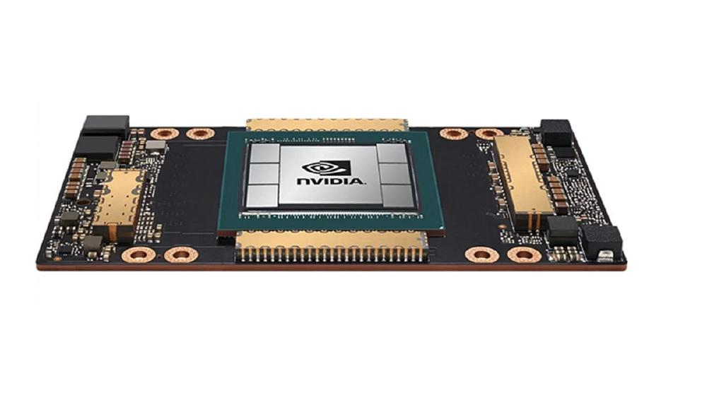
The NVIDIA A100 is the GPU that built the modern AI industry. Launched in May 2020 on the Ampere architecture, it was the first datacenter GPU designed from the ground up for the transformer era. Every major foundation model trained between 2020 and 2023 - GPT-3, PaLM, LLaMA, Chinchilla, Falcon - ran on clusters of A100s. The 80GB SXM variant, released later in 2020, doubled the memory of the original 40GB version and remains the reference configuration most people mean when they say "A100."
The A100 introduced several technologies that became standard across the industry: Multi-Instance GPU (MIG) for partitioning a single GPU into up to seven isolated instances, structural sparsity support for 2x inference throughput on compatible models, and third-generation NVLink with 600 GB/s of GPU-to-GPU bandwidth. These were not incremental improvements - they fundamentally changed how datacenters deployed GPU compute for AI workloads.
In 2026, the A100 is no longer the performance leader. The H100 delivers roughly 6x the FP8 throughput, and the B200 pushes that to over 15x. But the A100 remains the most widely deployed AI GPU on the planet, and its massive installed base means it is still the default choice for many production inference workloads, fine-tuning jobs, and research experiments. The secondary market is liquid and well-established, with 80GB SXM units trading between $10,000 and $15,000 - a fraction of their original ~$15,000-$20,000 MSRP.
Key Specifications
| Specification | Details |
|---|---|
| Manufacturer | NVIDIA |
| Architecture | Ampere (GA100) |
| Process Node | TSMC 7N |
| Transistors | 54.2 billion |
| Die Size | 826 mm² |
| CUDA Cores | 6,912 |
| Tensor Cores | 432 (3rd generation) |
| Streaming Multiprocessors | 108 |
| GPU Memory | 80 GB HBM2e |
| Memory Bandwidth | 2,039 GB/s (2.0 TB/s) |
| Memory Bus Width | 5,120-bit |
| L2 Cache | 40 MB |
| FP64 Performance | 9.7 TFLOPS (19.5 TFLOPS with sparsity) |
| FP32 Performance | 19.5 TFLOPS (39 TFLOPS with sparsity) |
| TF32 Performance | 156 TFLOPS (312 TFLOPS with sparsity) |
| FP16 / BF16 Performance | 312 TFLOPS (624 TFLOPS with sparsity) |
| INT8 Performance | 624 TOPS (1,248 TOPS with sparsity) |
| FP8 Support | No |
| NVLink | 3rd generation, 600 GB/s |
| PCIe | Gen 4.0 x16 |
| Multi-Instance GPU | Up to 7 instances |
| TDP | 400W (SXM), 300W (PCIe) |
| Form Factor | SXM4, PCIe |
| Cooling | Passive (SXM), Passive (PCIe) |
| Release Date | May 2020 (40GB), November 2020 (80GB) |
The GA100 die is one of the largest monolithic GPU dies ever manufactured. At 826 mm² on TSMC's 7N process (a custom variant of TSMC's N7 node), it approaches the reticle limit of the photolithography equipment. The full GA100 die contains 128 SMs, but the A100 product ships with 108 SMs enabled - a common yield optimization that allows NVIDIA to salvage dies with a limited number of defective SMs.
Each SM contains 64 FP32 CUDA cores and 4 third-generation Tensor Cores, giving the full GPU 6,912 CUDA cores and 432 Tensor Cores. The third-generation Tensor Cores added support for BF16 (bfloat16) and TF32 (TensorFloat-32) - precision formats that became essential for training large neural networks. TF32 in particular was a breakthrough: it provides the range of FP32 with the precision of FP16, enabling researchers to switch from FP32 training to TF32 with a single flag change and no accuracy loss. This is the kind of practical engineering decision that made the A100 the default training GPU for three years.
The 40 MB L2 cache is another often-overlooked specification. NVIDIA doubled the L2 cache from the V100's 6 MB to the A100's 40 MB, which significantly reduces HBM accesses for workloads with reusable data. For inference workloads where the same weights are accessed repeatedly across batch elements, the larger L2 cache provides a meaningful latency reduction that does not show up in peak FLOPS benchmarks but matters in real-world throughput.
Performance Benchmarks
| Metric | A100 80GB SXM | H100 SXM | H200 | B200 |
|---|---|---|---|---|
| FP16 Tensor TFLOPS | 312 (624 sparse) | 989 (1,979 sparse) | 989 (1,979 sparse) | 2,250 (4,500 sparse) |
| FP8 Tensor TFLOPS | N/A | 3,958 | 3,958 | 9,000 (dense) |
| INT8 TOPS | 624 (1,248 sparse) | 3,958 | 3,958 | 9,000 |
| Memory | 80 GB HBM2e | 80 GB HBM3 | 141 GB HBM3e | 192 GB HBM3e |
| Memory Bandwidth | 2,039 GB/s | 3,350 GB/s | 4,800 GB/s | 8,000 GB/s |
| TDP | 400W | 700W | 700W | 1,000W |
| NVLink Bandwidth | 600 GB/s | 900 GB/s | 900 GB/s | 1,800 GB/s |
| Interconnect Gen | 3rd gen NVLink | 4th gen NVLink | 4th gen NVLink | 5th gen NVLink |
| Transistors | 54.2B | 80B | 80B | 208B |
| Process | TSMC 7N | TSMC 4N | TSMC 4N | TSMC 4NP |
The raw numbers tell a clear story: each generation roughly doubles the compute and bandwidth of its predecessor. The A100's 312 TFLOPS of FP16 was groundbreaking in 2020, but the H100's introduction of FP8 at 3,958 TFLOPS changed the game entirely. For FP8-compatible inference workloads, an H100 delivers roughly 6x the throughput of an A100 at 1.75x the power draw.
But performance-per-dollar is where the A100 still competes. At $10,000-$15,000 on the secondary market versus $25,000-$30,000 for an H100, the A100 delivers meaningful compute at a significantly lower capital expenditure. For workloads that do not benefit from FP8 precision - or for organizations running models that were trained and optimized on Ampere - the A100 remains a rational choice.
Real-World Training Performance
On large language model training, the A100's real-world throughput depends heavily on the training framework, precision format, and parallelism strategy. Using Megatron-LM with tensor parallelism across 8 A100s in a DGX A100 node, a typical 7B-parameter model trains at approximately 3,000-4,000 tokens per second per GPU at BF16 precision. For comparison, the H100 achieves approximately 8,000-12,000 tokens per second per GPU on the same model at FP8 - a 2.5-3x improvement in practice, somewhat less than the theoretical peak ratio suggests.
The gap between theoretical peaks and real-world training throughput on the A100 is primarily driven by memory bandwidth limitations. At BF16 precision, the A100's Tensor Cores can deliver 312 TFLOPS, but the 2,039 GB/s of HBM2e bandwidth cannot keep up with the compute demand during the bandwidth-intensive phases of transformer training (attention, layer norms, activations). The Tensor Cores spend a significant fraction of their time waiting for data. This "arithmetic intensity" bottleneck is less severe on the H100 and H200, where higher bandwidth narrows the gap between peak and sustained performance.
Real-World Inference Performance
For inference, the A100's performance story is more nuanced. On batch-1 autoregressive inference (the typical interactive chatbot scenario), the A100 is almost entirely memory-bandwidth-bound. The throughput for generating output tokens is approximately bandwidth / (2 * parameters_in_bytes). For a 7B FP16 model, that works out to roughly 145 tokens per second on a single A100 - a respectable number that is adequate for single-user interactive applications.
At higher batch sizes, the A100 becomes more compute-bound and its Tensor Cores contribute more to throughput. Batch-32 inference on a 7B model can achieve over 2,000 tokens per second aggregate throughput, at which point the A100's compute resources are better utilized. For inference serving at scale, where requests are batched dynamically using techniques like continuous batching (vLLM, TensorRT-LLM), the A100 can be surprisingly efficient.
The INT8 path is the A100's best option for maximizing inference throughput. At 1,248 TOPS with sparsity, INT8 quantized inference can deliver roughly 2x the throughput of FP16 for models that quantize cleanly. The SmoothQuant and GPTQ quantization methods work well on most 7B-30B models when deployed on A100s, and INT8 inference with TensorRT-LLM is well-optimized for Ampere. The lack of FP8 support means the A100 misses the sweet spot between FP16 and INT8 - where the H100 operates most efficiently - but INT8 remains a viable alternative for production workloads.
Key Capabilities
Multi-Instance GPU (MIG). The A100 introduced MIG, which allows a single GPU to be partitioned into up to seven isolated GPU instances. Each instance gets its own dedicated memory, cache, and compute resources with full hardware isolation. This is not a software hack - it is a hardware feature that guarantees quality of service. For inference serving where multiple small models need to run concurrently on shared hardware, MIG eliminates the need to overprovision. A single A100 can serve seven different models simultaneously without any one workload impacting the others.
MIG partitions come in predefined profiles that allocate different amounts of memory and compute. The largest profile (1g.10gb on the 80GB variant gives ~10GB per instance with 1/7th of the compute) is suitable for small models and lightweight inference tasks. The full GPU can be split into various combinations: 7x 1g.10gb, 3x 2g.20gb + 1x 1g.10gb, 2x 3g.40gb, or 1x 7g.80gb (the whole GPU). This flexibility makes MIG particularly valuable for cloud providers who need to sell fractional GPU access with performance guarantees.
Structural Sparsity. The A100 was the first GPU to support structured sparsity acceleration in hardware. By exploiting the natural sparsity patterns in neural network weights - where many parameters are zero or near-zero - the third-generation Tensor Cores can deliver up to 2x throughput on compatible models. The 2:4 sparsity pattern (two out of every four values must be zero) is restrictive, and not all models can be pruned to fit it without accuracy loss. But for models that can, the effective throughput doubles across all precisions. This feature became standard in Hopper and Blackwell.
In practice, the adoption of structural sparsity has been slower than NVIDIA hoped. The 2:4 pattern requires careful fine-tuning after pruning to recover accuracy, and many model developers prefer the simplicity of dense computation over the engineering effort of sparsity optimization. However, for production deployments where inference cost is the primary concern, sparsity can provide meaningful savings. NVIDIA's ASP (Automatic SParsity) toolkit makes it straightforward to prune and fine-tune models for 2:4 sparsity on Ampere hardware.
Third-Generation NVLink. With 12 NVLink 3.0 links providing 600 GB/s of bidirectional bandwidth, the A100 supports efficient multi-GPU training across up to 16 GPUs via NVSwitch. This was a 2x bandwidth improvement over the V100's NVLink 2.0 and enabled the large-scale distributed training runs that produced the first generation of frontier language models. The bandwidth is modest by 2026 standards - the B200 offers 1,800 GB/s via NVLink 5 - but it remains adequate for many multi-GPU inference and fine-tuning setups.
The DGX A100 system used NVSwitch to create an all-to-all NVLink fabric among its 8 GPUs, providing 600 GB/s bidirectional bandwidth between any pair of GPUs. For training runs that span multiple DGX nodes, communication falls back to InfiniBand (typically 200 Gb/s HDR or 400 Gb/s NDR), which is an order of magnitude slower than NVLink. This InfiniBand bottleneck at the node boundary is the primary scaling limitation for A100 clusters and was one of the key problems the H100's NVLink Switch System was designed to address.
TF32 Precision Format. While not a hardware feature in the same sense as MIG or sparsity, the TF32 precision format introduced with the A100 deserves specific mention. TF32 uses 19 bits (1 sign + 8 exponent + 10 mantissa) and provides the dynamic range of FP32 with the throughput of FP16. The A100's Tensor Cores accelerate TF32 math at the same rate as FP16 - 312 TFLOPS dense - which means training workflows that previously ran at FP32 speeds (19.5 TFLOPS) could immediately run at 16x the throughput without any code changes, just by enabling TF32 mode (which NVIDIA made the default in PyTorch and TensorFlow). This single change probably saved more collective GPU-hours across the industry than any other A100 feature.
Architecture Deep Dive
Memory Subsystem
The A100's memory subsystem uses five stacks of HBM2e, each providing approximately 410 GB/s of bandwidth for a total of 2,039 GB/s. The HBM2e stacks communicate with the GPU die through a 5,120-bit memory bus. Each stack connects to one of five memory partition controllers on the GPU die, and the 40 MB L2 cache is distributed across these five partitions.
The L2 cache architecture deserves attention. The A100 increased the L2 from the V100's 6 MB to 40 MB - a 6.7x increase - and added "cache residency controls" that allow programmers to specify which data should be prioritized for L2 caching. For inference workloads where model weights are accessed repeatedly across a batch, keeping hot weights in L2 can reduce effective memory latency by 3-5x compared to HBM accesses. This is one of the reasons the A100's real-world inference performance often exceeds what bandwidth-limited roofline models predict.
Compute Architecture
The A100's 108 SMs are organized into 8 GPCs (GPU Processing Clusters), each containing up to 16 SMs via TPCs (Texture Processing Clusters). Each SM contains 64 FP32 CUDA cores, 64 INT32 cores, 4 third-generation Tensor Cores, and 4 texture units. The Tensor Cores support FP16, BF16, TF32, FP64, INT8, INT4, and binary (INT1) precisions.
The third-generation Tensor Cores process 256 FP16 multiply-and-accumulate operations per clock cycle per Tensor Core. With 432 Tensor Cores running at the A100's ~1.4 GHz boost clock, this produces the 312 TFLOPS FP16 peak. The Tensor Cores operate on small matrix tiles (typically 16x16 or 16x8 depending on the precision), and the CUDA programming model exposes them through the WMMA (Warp Matrix Multiply-Accumulate) API or, more commonly, through libraries like cuBLAS and cuDNN that map higher-level operations onto Tensor Core instructions.
Form Factor Variants
The A100 ships in two form factors: SXM4 and PCIe. The SXM4 variant is designed for NVIDIA's DGX and HGX platforms, where it plugs into a baseboard with NVSwitch connectivity and a robust power delivery system supporting 400W TDP. The PCIe variant is a standard full-height, full-length dual-slot card that fits in any PCIe Gen 4 server, but with a reduced 300W TDP and without NVLink (or with limited NVLink in some configurations).
For AI training at scale, the SXM variant is effectively mandatory - the NVLink connectivity and higher power limit are essential for multi-GPU training efficiency. The PCIe variant is more commonly used for inference, development, and HPC workloads where a single GPU or a pair of GPUs is sufficient and the host server does not support SXM baseboards.
Pricing and Availability
The A100 has the most mature and liquid secondary market of any AI GPU. Original MSRPs ranged from $10,000 to $15,000 for the PCIe variant and $15,000 to $20,000 for the SXM variant when new. In the current secondary market, 80GB SXM units typically trade between $10,000 and $15,000, with PCIe variants available for $8,000 to $12,000.
| Configuration | Estimated Price (2026) |
|---|---|
| A100 80GB SXM (used) | $10,000 - $15,000 |
| A100 80GB PCIe (used) | $8,000 - $12,000 |
| A100 40GB SXM (used) | $5,000 - $8,000 |
| DGX A100 (8x A100 80GB, used) | $80,000 - $120,000 |
| Cloud rental (per GPU hour) | $1.50 - $3.00 |
Cloud availability remains excellent. Every major cloud provider - AWS (p4d instances), GCP (a2-highgpu), Azure (ND A100 v4), OCI, Lambda, CoreWeave - offers A100 instances, and spot pricing can be significantly lower than on-demand rates. The A100 is the most affordable datacenter GPU available in the cloud, making it the default choice for cost-sensitive workloads.
The supply situation is the inverse of newer GPUs. While B200 and GB200 NVL72 allocations remain constrained, A100 inventory is abundant. Organizations looking to scale inference clusters quickly can procure A100s with minimal lead time, which is a meaningful operational advantage over waiting months for Blackwell allocations.
Total Cost of Ownership
The A100's 400W TDP gives it a significant operational cost advantage over newer GPUs. At a typical datacenter power cost of $0.10/kWh with a PUE (Power Usage Effectiveness) of 1.3, a single A100 costs approximately $456 per year in electricity. An H100 at 700W costs approximately $798 per year, and a B200 at 1,000W costs approximately $1,140 per year. Over a three-year deployment, the A100 saves roughly $1,000-$2,000 per GPU in power costs alone compared to Hopper and Blackwell.
When you factor in the lower acquisition cost ($10,000-$15,000 used versus $25,000+ new for H100), the A100 can deliver a lower three-year total cost of ownership for workloads where its performance is sufficient. The key question is whether the workload benefits enough from FP8 or FP4 precision to justify the higher capital and operational cost of newer hardware. For many inference workloads - particularly those serving quantized 7B-13B models to moderate traffic - the answer is no.
Strengths
- Most widely deployed AI GPU in the world - massive ecosystem of optimized software, libraries, and deployment tooling
- Mature and liquid secondary market with predictable pricing at $10,000-$15,000 for 80GB SXM units
- 400W TDP is significantly more power-efficient than the 700W H100 or 1,000W B200, reducing datacenter cooling and power costs
- Multi-Instance GPU (MIG) enables hardware-isolated multi-tenant inference on a single card
- Structural sparsity support delivers 2x throughput on compatible models across all precisions
- 80GB HBM2e is still sufficient for serving most production models, including quantized versions of 70B-parameter models
- Abundant cloud availability with the lowest per-hour rental costs of any datacenter GPU
- TF32 precision delivers 16x FP32 throughput with no code changes - the most impactful usability feature in datacenter GPU history
- 40 MB L2 cache significantly reduces HBM accesses for inference workloads with reusable data
Weaknesses
- No FP8 support - the single biggest performance gap versus Hopper and Blackwell, which deliver 4-6x more throughput at FP8 precision
- 2,039 GB/s memory bandwidth is a bottleneck for large language model inference where throughput is memory-bandwidth-bound
- 80GB memory capacity limits the size of models that can be served without multi-GPU sharding - not enough for unquantized 70B+ models
- PCIe Gen 4 interconnect (versus Gen 5 on H100+) limits host-to-device transfer speeds
- Third-generation NVLink at 600 GB/s is less than half the bandwidth of H100's fourth-generation NVLink (900 GB/s)
- No Transformer Engine - the hardware-accelerated dynamic precision switching that gives Hopper and Blackwell their edge on transformer workloads
- Aging TSMC 7N process delivers lower transistor density and efficiency compared to the 4N/4NP used in Hopper and Blackwell
- DGX A100 NVLink domain is limited to 8 GPUs per node - no NVLink Switch System support for scaling beyond a single node
- FP64 performance (9.7 TFLOPS dense) is adequate but not exceptional for HPC workloads that require double precision
Who Should Buy the A100 in 2026
The A100 is not the right GPU for everyone in 2026, but it remains the right GPU for a significant number of use cases. Here is a framework for evaluating whether the A100 makes sense for your workload.
Good Fit
Inference serving for 7B-13B models. If your production workload is serving quantized 7B or 13B models at moderate traffic (hundreds to low thousands of requests per second), the A100 delivers adequate throughput at the lowest capital cost. INT8 quantization on Ampere is mature and well-optimized, and the 80GB memory comfortably holds multiple quantized small models (or a single quantized 30B model with room for KV-cache).
Fine-tuning and LoRA training. For fine-tuning pre-trained models using LoRA or QLoRA, the A100's BF16 Tensor Core performance is more than sufficient. Fine-tuning does not require the FP8 Transformer Engine because the training runs are short (hours to days, not weeks to months) and the compute savings from FP8 do not justify the migration effort. The 80GB memory handles LoRA fine-tuning for models up to 70B parameters with appropriate quantization.
Research and experimentation. Academic and corporate research teams running experiments, hyperparameter sweeps, and prototype training on models up to 13B parameters will find the A100 more than adequate. The lower cloud rental cost ($1.50-$3.00 per GPU-hour versus $2.50-$4.50 for H100) translates to meaningful savings for research budgets.
Budget-constrained inference scaling. Organizations that need to scale inference capacity quickly and cheaply can deploy A100s from the secondary market with minimal lead time. The $10,000-$15,000 price point per GPU allows larger fleet sizes for the same budget, which matters when throughput is more important than per-GPU performance.
Poor Fit
Large-scale training (70B+ models). The A100's lack of FP8 support and lower bandwidth make it significantly less efficient for training large models. The H100 delivers 2.5-3x the training throughput per GPU at FP8, and the NVLink Switch System enables more efficient multi-node scaling. For training runs that consume millions of GPU-hours, the per-GPU performance difference translates to months of additional training time.
High-throughput inference at scale. If your inference fleet processes millions of tokens per day and latency is a competitive differentiator, the H100 or B200 will deliver more tokens per dollar per hour despite the higher GPU price. The FP8 path on Hopper and the FP4 path on Blackwell provide 3-5x more inference throughput per GPU.
Serving 70B+ models. The A100's 80GB memory is insufficient for unquantized 70B+ models. While INT8 quantization can fit a 70B model into 80GB, this leaves minimal memory for KV-cache, limiting concurrent requests. The H200 with 141GB of HBM3e is a much better choice for this workload.
Model Compatibility Guide
Understanding which models fit on the A100 is critical for deployment planning. The following table shows memory requirements for popular model families at different precisions.
| Model | FP16 Size | INT8 Size | Fits on A100 80GB (FP16)? | Fits on A100 80GB (INT8)? | KV-Cache Headroom (INT8) |
|---|---|---|---|---|---|
| Llama 3 8B | ~16 GB | ~8 GB | Yes | Yes | ~72 GB |
| Mistral 7B | ~14 GB | ~7 GB | Yes | Yes | ~73 GB |
| Llama 3 70B | ~140 GB | ~70 GB | No | Tight (no KV room) | ~10 GB |
| Qwen 2.5 72B | ~144 GB | ~72 GB | No | Tight (no KV room) | ~8 GB |
| Mixtral 8x7B | ~93 GB | ~47 GB | No | Yes | ~33 GB |
| Llama 3 13B | ~26 GB | ~13 GB | Yes | Yes | ~67 GB |
| Code Llama 34B | ~68 GB | ~34 GB | Yes (tight) | Yes | ~46 GB |
The "KV-Cache Headroom" column shows how much memory remains for KV-cache after loading model weights. This determines how many concurrent requests the GPU can handle and the maximum context length per request. For production inference serving with continuous batching, 20-40 GB of KV-cache headroom is typically sufficient for moderate batch sizes with 4K-8K context windows.
Generational Comparison
Understanding where the A100 sits relative to its successors and how each generation addresses different bottlenecks helps frame purchasing decisions.
A100 vs H100: The FP8 Question
The H100 delivers approximately 3x the training throughput and 2.5-3.5x the inference throughput of the A100 for transformer workloads. The dominant factor is FP8 support: the H100's Transformer Engine enables FP8 training and inference that the A100 simply cannot do.
For workloads that can operate at INT8, the A100 narrows the gap. The A100 delivers 1,248 TOPS INT8 with sparsity, which is roughly one-third of the H100's 3,958 TFLOPS FP8. The cost ratio is roughly 1:2 (A100 at $10K-$15K used vs H100 at $25K-$30K new), so on a price-adjusted basis, the A100 delivers approximately 60-70% of the H100's INT8/FP8 performance per dollar. That ratio makes the A100 competitive for cost-sensitive INT8 inference workloads.
A100 vs H200: Memory as the Differentiator
The H200 does not improve compute over the H100 but delivers 76% more memory and 43% more bandwidth. Compared to the A100, the H200 provides 1.76x memory capacity, 2.35x bandwidth, and the FP8 Transformer Engine. The H200 is strictly superior to the A100 in every dimension - the only argument for the A100 is price.
At $10K-$15K (A100 used) versus $25K-$35K (H200 new), the A100 costs 40-60% as much. For workloads that fit in 80GB and do not benefit from FP8, this cost difference makes the A100 the economically rational choice.
A100 vs B200: Two Generations Apart
The B200 represents a full two-generation leap over the A100. At FP4, the B200 delivers approximately 18,000 TFLOPS sparse - roughly 29x the A100's 624 TFLOPS FP16 sparse. The memory capacity is 2.4x larger (192GB vs 80GB) and bandwidth is 3.9x higher (8,000 vs 2,039 GB/s). At $30K-$40K versus $10K-$15K, the B200 costs approximately 2.5x as much but delivers 15-29x the throughput depending on precision format. The B200 is the clear winner on price-performance for any workload that can use FP4 or FP8.
Software Ecosystem
The A100's greatest competitive advantage in 2026 may be its software ecosystem rather than its hardware specifications. Five years of optimization have produced deeply tuned implementations across every major framework and inference engine.
Training Frameworks. PyTorch, TensorFlow, JAX, and Megatron-LM all have mature, well-tested A100 code paths. The Ampere architecture's CUDA compute capability (8.0) is supported by every major training framework, and performance-critical kernels (attention, GEMM, LayerNorm) have been hand-optimized for Ampere's SM architecture. These optimizations accumulated over years of real-world production use and represent a significant amount of engineering effort that has not been replicated to the same degree on newer architectures.
Inference Engines. TensorRT-LLM, vLLM, and text-generation-inference all support A100 with well-optimized INT8 paths. The A100's INT8 Tensor Core performance is fully exploited by these engines, and the quantization workflows (GPTQ, AWQ, SmoothQuant) are mature and well-documented for Ampere deployment.
CUDA Library Support. cuBLAS, cuDNN, cuFFT, NCCL, and the full CUDA toolkit are deeply optimized for compute capability 8.0. The A100 has the longest support history of any current-generation GPU, which means edge cases, bugs, and performance regressions have been identified and fixed over five years of production use. This stability is valuable for production deployments where reliability matters more than peak performance.
Container and Orchestration Support. The A100 is fully supported by NVIDIA's container toolkit, Kubernetes device plugin, GPU operator, and every major container orchestration platform. MIG is natively integrated with Kubernetes for fine-grained GPU scheduling. Monitoring and telemetry tools (DCGM, nvidia-smi, Prometheus exporters) are mature and reliable.
Use Case Deep Dives
Fine-Tuning Large Language Models
The A100 remains an excellent GPU for fine-tuning pre-trained models using parameter-efficient methods like LoRA and QLoRA. A single A100 80GB can fine-tune models up to 70B parameters using QLoRA (4-bit base model with LoRA adapters in BF16).
Typical fine-tuning performance on A100 80GB:
| Model Size | Method | Batch Size | Throughput (samples/sec) | Memory Usage |
|---|---|---|---|---|
| 7B | Full fine-tune (BF16) | 4 | ~8 | ~60 GB |
| 7B | LoRA (BF16) | 8 | ~15 | ~20 GB |
| 13B | LoRA (BF16) | 4 | ~8 | ~35 GB |
| 70B | QLoRA (4-bit + BF16) | 1 | ~1.5 | ~45 GB |
For academic researchers and smaller companies, the A100's combination of adequate fine-tuning performance and low cloud rental cost ($1.50-$3.00/hour) makes it the most cost-effective option. A full QLoRA fine-tuning run on a 7B model with 50,000 samples typically completes in 2-4 hours on a single A100, costing $3-$12 in cloud compute.
Inference Serving at Scale
For organizations running inference serving clusters with 10-100 GPUs, the A100 provides a compelling economic profile. Consider a fleet of 32 A100 80GB GPUs serving a quantized 7B model with INT8 precision:
- Per-GPU throughput: ~300 tokens/sec at batch-8 with INT8
- Fleet throughput: ~9,600 tokens/sec aggregate
- GPU cost: 32 x $12,500 = $400,000 (used market)
- Annual power cost: 32 x $456 = $14,592
- Cloud equivalent: 32 x $2.00/hr x 8,760 hrs = $560,640/year
At these numbers, buying used A100s pays for itself in under 9 months compared to cloud rental at $2/GPU-hour. The low per-GPU cost and mature software ecosystem make the A100 the most practical choice for organizations building their first on-premises inference cluster.
Scientific Computing and HPC
While the A100 is primarily discussed in the context of AI, it remains a capable HPC accelerator. The 19.5 TFLOPS FP64 peak (39 TFLOPS with sparsity) and 2,039 GB/s memory bandwidth make it competitive for computational fluid dynamics, molecular dynamics, weather modeling, and other FP64-intensive workloads.
The A100's third-generation Tensor Cores support FP64 matrix operations, which was a first for NVIDIA datacenter GPUs. This enables mixed-precision HPC workflows where compute-intensive portions use TF32 or FP64 Tensor Cores while data movement uses lower precision. For HPC applications that can tolerate TF32 precision (which maintains FP32 dynamic range), the A100 delivers 156 TFLOPS - an 8x improvement over FP64.
Cloud Provider Availability
The A100 is available from every major and most minor cloud providers, making it the most accessible datacenter GPU in the cloud. Here is a summary of A100 instance availability:
| Cloud Provider | Instance Type | GPUs per Instance | On-Demand Price (approx.) |
|---|---|---|---|
| AWS | p4d.24xlarge | 8x A100 40GB | ~$32/hr |
| AWS | p4de.24xlarge | 8x A100 80GB | ~$40/hr |
| Google Cloud | a2-highgpu-1g | 1x A100 40GB | ~$3.70/hr |
| Google Cloud | a2-ultragpu-8g | 8x A100 80GB | ~$40/hr |
| Microsoft Azure | ND A100 v4 | 8x A100 80GB | ~$33/hr |
| Oracle Cloud | BM.GPU4.8 | 8x A100 40GB | ~$25/hr |
| Lambda Cloud | gpu_8x_a100_80gb | 8x A100 80GB | ~$15/hr |
| CoreWeave | A100 80GB | 1-8x A100 80GB | ~$2.10/hr/GPU |
Spot and preemptible pricing can be 50-70% lower than on-demand rates, making the A100 exceptionally affordable for batch workloads and development. The wide availability across providers also gives buyers negotiating leverage - competitive cloud pricing for A100 instances is well-established.
For organizations running cost-optimized inference, the A100's cloud pricing is difficult to beat. At $2-3 per GPU-hour for a single A100 80GB, a month of continuous operation costs $1,440-$2,160 - less than 15% of the GPU's secondary market purchase price. This makes cloud rental the preferred option for workloads with variable or growing compute demand, while on-premises deployment makes sense for sustained, predictable workloads where a 9-12 month payback period is acceptable.
Export Control and Compliance
The A100's availability has been affected by US export controls targeting advanced AI chips. Since October 2022, export of A100 GPUs to China, Russia, and certain other countries has been restricted. This has created a bifurcated market where A100s command premium prices in regions subject to export controls.
For organizations operating in affected regions, NVIDIA offers the A800 - an export-compliant variant of the A100 with reduced NVLink bandwidth (400 GB/s versus 600 GB/s) and slightly lower compute performance. The A800 is architecturally identical to the A100 but with artificial performance caps that bring it below the export control thresholds.
Organizations purchasing A100s should verify compliance with applicable export control regulations, particularly for deployments in cloud environments that serve customers in restricted jurisdictions. The compliance landscape continues to evolve, and purchasing decisions should account for potential future restrictions.
The A100's Enduring Relevance
The A100's longevity in the datacenter GPU market is remarkable. Launched in May 2020, it remains actively deployed and commercially relevant six years later. This staying power stems from three factors:
Installed base momentum. When thousands of organizations have built their AI infrastructure around A100s - with optimized code, trained models, established operational procedures, and amortized capital costs - switching to a new GPU architecture carries real costs beyond the hardware price. The migration effort, validation testing, and operational risk of transitioning to Hopper or Blackwell is non-trivial, and many organizations rationally choose to continue operating their A100 fleets until the hardware reaches end-of-life.
The "good enough" threshold. For many AI workloads, the A100's performance is not just adequate - it is more than sufficient. A single A100 can serve a quantized 7B model at hundreds of tokens per second, fine-tune models with LoRA in hours, and run research experiments at reasonable speed. Not every workload needs FP8 at 3,958 TFLOPS. The A100's 312 TFLOPS at FP16 is still a lot of compute by any measure, and for workloads that do not push against its limits, the performance headroom of newer GPUs goes unused.
Economic rationality. At $10,000-$15,000 on the secondary market, the A100 offers the lowest cost per GPU of any datacenter-grade AI accelerator. For budget-constrained organizations - universities, startups, small companies, and research labs - the A100 provides access to meaningful AI compute at an accessible price point. The alternative is not "buy an H100 instead" but "cannot afford AI compute at all." In this context, the A100 is not a compromise - it is an enabler.
Related Coverage
- NVIDIA H100 - The AI Training Benchmark - The Hopper successor that introduced FP8 and the Transformer Engine
- NVIDIA H200 - Inference-Optimized Hopper - More memory and bandwidth on the same Hopper architecture
- NVIDIA B200 - Blackwell Flagship GPU - The current-generation flagship with 9,000 TFLOPS FP8
- NVIDIA GB200 NVL72 - Rack-Scale Blackwell - 72-GPU rack system delivering 1,440 PFLOPS FP4
- NVIDIA GB300 NVL72 - Blackwell Ultra - Next-generation rack system with 288GB HBM3e per GPU
Sources
