Microsoft Maia 200 - Azure's Inference Accelerator
Microsoft Maia 200 specs, benchmarks, and architecture analysis. TSMC 3nm, 216GB HBM3e, 10 PFLOPS FP4, 750W - Microsoft's first inference-only silicon deployed in Azure.
Overview
Microsoft's Maia 200, announced January 26, 2026, is the company's second-generation custom AI accelerator and its first silicon platform built specifically for large-scale inference rather than general-purpose AI training. Maia 200 runs inside Azure's US Central datacenter in Des Moines, Iowa today, with US West 3 in Phoenix next in line, and further regions expanding through 2026.
TL;DR
- Inference-only ASIC on TSMC 3nm with 216GB HBM3e at 7 TB/s and 272MB on-chip SRAM
- Claims 10+ PFLOPS FP4 and 5+ PFLOPS FP8 in a 750W envelope - currently powering GPT-class models on Azure
- 3x the FP4 throughput of AWS Trainium3 and higher FP8 than Google TPU v7 Ironwood, by Microsoft's own numbers
- Inference only - not rolled out for training workloads
The chip arrived as Microsoft's answer to growing internal infrastructure costs and continued dependency on NVIDIA GPUs for serving OpenAI models at Azure scale. Maia 200 runs on a custom Ethernet-based interconnect rather than NVLink or InfiniBand, reflecting a deliberate architectural choice to scale horizontally with standard networking fabric instead of proprietary GPU interconnects. Each accelerator provides 2.8 TB/s bidirectional bandwidth to its peers via an on-die NIC.
With 140 billion transistors and a tile-based micro-architecture, Maia 200 is meaningfully more complex than the original Maia 100 rolled out in 2023. Microsoft says the chip delivers 30% better performance per dollar than the previous hardware generation already running in its fleet.
Key Specifications
| Specification | Details |
|---|---|
| Manufacturer | Microsoft |
| Product Family | Maia |
| Chip Type | ASIC (Inference) |
| Process Node | TSMC N3 (3nm) |
| Transistors | 140 billion |
| Memory | 216GB HBM3e |
| Memory Bandwidth | 7,000 GB/s (7 TB/s) |
| On-chip SRAM | 272MB (CSRAM + TSRAM) |
| FP8 Performance | >5,000 TFLOPS (5 PFLOPS) |
| FP4 Performance | >10,000 TFLOPS (10.1 PFLOPS) |
| BF16 Performance | Not disclosed |
| TDP | 750W |
| Scale-up Interconnect | Custom Ethernet, 2.8 TB/s bidirectional per chip |
| Max Cluster Size | 6,144 accelerators |
| Target Workload | Inference only |
| Release Date | January 2026 |
Performance Benchmarks
No independent third-party benchmarks are available yet. All performance data comes from Microsoft's own announcements. The table below summarizes the vendor-reported figures against the two closest hyperscaler competitors:
| Benchmark | Maia 200 | AWS Trainium3 | Google TPU v7 Ironwood |
|---|---|---|---|
| FP4 Performance | >10 PFLOPS | ~3.4 PFLOPS (est.) | Not disclosed |
| FP8 Performance | >5 PFLOPS | ~2.5 PFLOPS | ~4.7 PFLOPS (est.) |
| Memory Capacity | 216GB HBM3e | 144GB HBM3e | 192GB HBM per pod chip |
| Memory Bandwidth | 7 TB/s | ~4 TB/s | ~7.4 TB/s |
| TDP | 750W | ~600W | ~900W (est.) |
| Max Cluster | 6,144 chips | 65,536 chips | 9,216 chips per pod |
Microsoft's FP4 comparison against Trainium3 is the most specific claim: "three times the FP4 performance." The FP8 vs. TPU v7 comparison is vaguer - "above Google's seventh generation TPU" with no specific multiplier cited. Both comparisons rely on vendor-supplied figures. The Trainium3 comparison is more credible because AWS has published its own FP8 numbers; the TPU v7 comparison rests on Google's undisclosed FP8 figure.
What's clear from the architecture alone: the 7 TB/s HBM3e bandwidth is sizable. NVIDIA's B200 reaches 8 TB/s on 192GB. Maia 200 gives up some bandwidth density but gains 24GB of capacity, which matters for serving large models with long context.
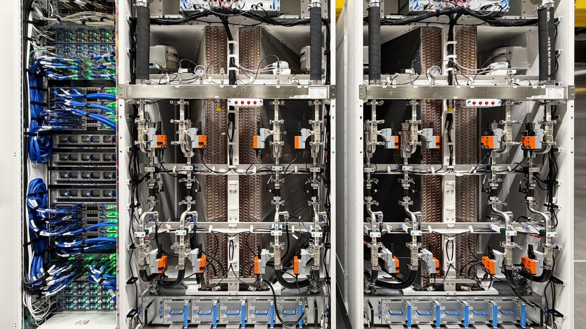 Maia 200 accelerators installed in Azure datacenter racks with liquid cooling sidecars.
Source: news.microsoft.com
Maia 200 accelerators installed in Azure datacenter racks with liquid cooling sidecars.
Source: news.microsoft.com
Key Capabilities
Tile-Based Compute Architecture
Maia 200 uses a hierarchical tile design. Each tile pairs a Tile Tensor Unit (TTU) with a Tile Vector Processor (TVP). The TTU handles high-throughput matrix multiply and convolution in FP8, FP6, and FP4, including mixed-precision modes like FP8 activations multiplied by FP4 weights. The TVP is a fully programmable SIMD engine supporting FP8, BF16, FP16, and FP32 for operations that need higher precision. A lightweight Tile Control Processor (TCP) coordinates both.
The FP4 throughput is 2x that of FP8 and 8x that of BF16 on the same die, which is why Microsoft positions Maia 200 specifically for modern reasoning and large language models where FP4 quantization is becoming standard practice.
Three-Tier Memory Subsystem
The 272MB on-chip SRAM divides into two software-managed layers: Cluster SRAM (CSRAM) and Tile SRAM (TSRAM). Both are fully deterministic - the compiler places data explicitly rather than relying on hardware caches. This is the same approach Groq uses in its LPU architecture, and for the same reason: deterministic latency for inference, no cache thrash, no unpredictable bandwidth spikes. Behind the SRAM sits 216GB of HBM3e at 7 TB/s.
Data movement between all three tiers is handled by a custom Network-on-Chip with hierarchical DMA engines at the tile, cluster, and network levels. Microsoft also built a custom AI Transport Layer (ATL) for chip-to-chip communication, supporting packet spraying and multipath routing to minimize congestion at cluster scale.
Ethernet-Based Scale-Up
Microsoft explicitly chose standard Ethernet over proprietary interconnects like NVLink or Intel Gaudi's HCCL. Each Maia 200 has an on-die NIC providing 1.4 TB/s unidirectional bandwidth. The first tier of the topology uses a "Fully Connected Quad" (FCQ): four accelerators connected via direct switchless links. The second tier extends this to 6,144 accelerators. This architecture is harder to beat on raw GPU-to-GPU bandwidth compared to NVLink, but it gives Microsoft full control of the networking stack and avoids licensing proprietary interconnects.
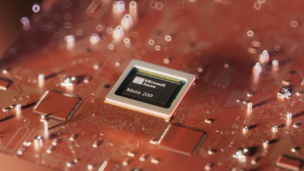
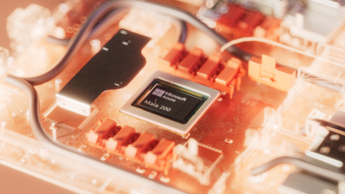 The Maia 200 silicon die, showing 140 billion transistors on TSMC N3.
Source: news.microsoft.com
The Maia 200 silicon die, showing 140 billion transistors on TSMC N3.
Source: news.microsoft.com
Pricing and Availability
Maia 200 is not available for external purchase or cloud rental at a per-chip level. Microsoft uses it exclusively for internal Azure inference workloads, mainly serving OpenAI's production models. There's no announced Azure VM SKU or dedicated pricing for Maia 200 instances as of April 2026.
This differs from Google's approach with Cloud TPUs, where external customers can rent TPU v6e and TPU v7 pods. It also differs from AWS, where Trainium2 and Trainium3 are available as EC2 Trn instances.
Microsoft claims 30% better performance per dollar compared to its own existing hardware fleet, but doesn't disclose the baseline hardware or the specific model and batch size where that improvement holds. External validation of that number isn't possible without access to the systems.
Strengths and Weaknesses
Strengths
- High FP4 throughput (10.1 PFLOPS) relative to TDP for inference workloads
- Large 216GB HBM3e capacity serves 70B+ parameter models comfortably
- 272MB deterministic on-chip SRAM reduces memory latency for attention operations
- Scales to 6,144 chips in two-tier Ethernet topology without proprietary interconnects
- 140B transistors on TSMC N3 gives substantial room for future iterations
Weaknesses
- No independent benchmark data - all performance figures from vendor
- Inference-only: not usable for training workloads
- Not externally available - Azure customers cannot directly access Maia 200 resources
- No disclosed tokens-per-second figures on standard benchmarks like MLPerf
- Custom software stack (Maia Triton compiler, NPL) adds engineering overhead vs. CUDA ecosystem
Related Coverage
- AWS Trainium3 - Microsoft's primary FP4 comparison target
- Google TPU v7 Ironwood - The other hyperscaler chip Maia 200 claims to beat
- GPT-5.2 - Among the production models Microsoft runs on Maia 200 inside Azure
Sources
- Microsoft Official Blog: Maia 200 announcement
- Deep Dive into the Maia 200 Architecture - Microsoft Community Hub
- Tom's Hardware: Microsoft Introduces Maia 200
- The Register: Microsoft looks to drive down AI infra costs with Maia 200
- TechCrunch: Microsoft announces powerful new chip for AI inference
- NAND Research: Microsoft Azure Maia 200 Inference Accelerator
✓ Last verified April 1, 2026

