Meta MTIA 400: GenAI Inference at Scale
Meta's second-gen ASIC delivers 6 PFLOPS FP8 and 288 GB HBM for GenAI and recommendation inference inside Meta's data centers.
Overview
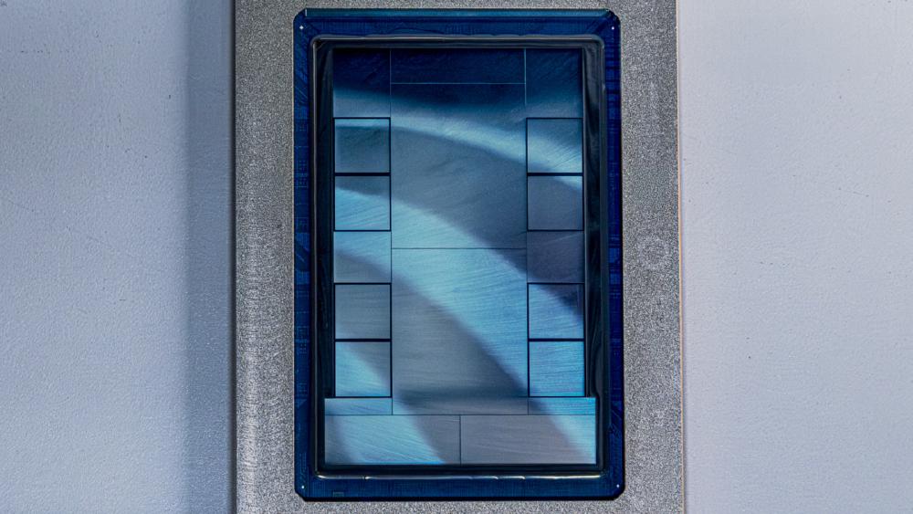
The MTIA 400 is Meta's second-generation custom ASIC for AI inference - a chip that exists entirely inside Meta's own data centers and can't be purchased, rented, or independently tested by anyone outside the company. Announced in March 2026 alongside the full four-chip MTIA roadmap, it doubles the compute chiplet count of its predecessor, the MTIA 300, and expands the target workload from ranking and recommendation (R&R) to include generative AI inference. At 6 PFLOPS FP8 and 288 GB HBM across a 72-chip rack-scale domain, the numbers look competitive on paper. The problem is that every one of those numbers comes from Meta.
There's no MLPerf submission, no independent benchmark, and no way to copy the claimed performance. What Meta calls "competitive with leading commercial products" probably means the H100/MI300X generation - not NVIDIA's Blackwell lineup, which was already shipping when the MTIA 400 announcement dropped. The MX4 number - 12 PFLOPS - sounds impressive but uses a Microscaling 4-bit format that isn't directly comparable to standard FP8 or FP16 PFLOPS figures from competing vendors. These distinctions matter when assessing whether MTIA 400 actually closes the gap with commercial AI accelerators.
Strategically, the chip is significant. Meta is the only source of these workloads, so Meta is the only judge of whether the chip succeeds. Given the company runs hundreds of millions of daily inference requests across Facebook, Instagram, WhatsApp, and an expanding suite of generative AI products, the scale of deployment will be enormous even if the chip never appears on a third-party benchmark.
TL;DR
- Meta's second-gen MTIA ASIC: 6 PFLOPS FP8, 288 GB HBM, 9.2 TB/s bandwidth, 1,200W TDP
- Two compute chiplets (doubled vs MTIA 300's one), plus dedicated network and HBM chiplets
- 12 PFLOPS MX4 figure uses Microscaling 4-bit format - not directly comparable to vendor FP8 numbers
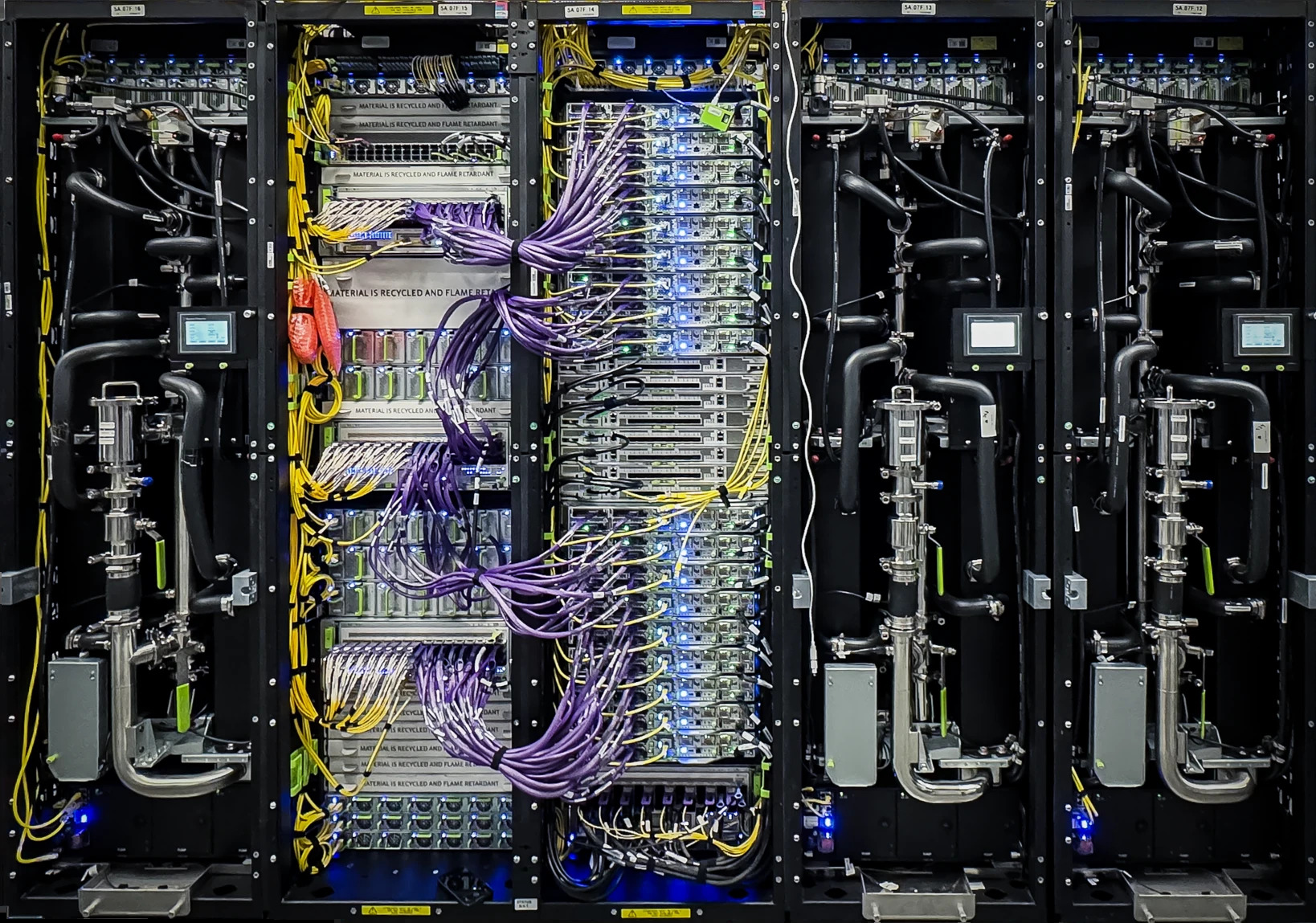
- 72-chip rack forms a single scale-up domain via switched backplane; 1.2 Tbps scale-up, 100 Gbps scale-out
- Expands beyond R&R into GenAI inference - image and video generation at Meta's scale
- Internal use only - no external sales, no cloud access, no independent benchmarks
- "Competitive with leading commercial products" likely means H100 generation, not Blackwell
 The MTIA 400 rack configuration: 72 chips per rack, connected via a switched backplane as a single scale-up domain.
Source: xpu.pub / Meta
The MTIA 400 rack configuration: 72 chips per rack, connected via a switched backplane as a single scale-up domain.
Source: xpu.pub / Meta
Key Specifications
| Specification | Details |
|---|---|
| Manufacturer | Meta Platforms |
| Co-developer | Broadcom |
| Fabrication | TSMC (process node not disclosed) |
| Product Family | MTIA (Meta Training and Inference Accelerator) |
| Chip Type | ASIC |
| Architecture | Two compute chiplets + network chiplets + HBM stacks (RISC-V vector) |
| FP8 / MX8 Performance | 6 PFLOPS (6,000 TFLOPS) |
| MX4 Performance | 12 PFLOPS (block-level shared exponent 4-bit format) |
| BF16 Performance | 3 PFLOPS |
| Memory | 288 GB HBM |
| Memory Bandwidth | 9.2 TB/s |
| TDP | 1,200W |
| Scale-up Networking | 1.2 Tbps |
| Scale-out Networking | 100 Gbps |
| Rack Config | 72 chips per rack, single scale-up domain (switched backplane) |
| Target Workloads | GenAI inference, Ranking & Recommendation |
| Status | Lab testing complete, deployment on track |
| Availability | Internal use only - not sold commercially |
The MTIA Roadmap
The MTIA 400 doesn't make much sense outside of Meta's larger silicon strategy. The company published a four-generation roadmap at the same time, covering chips every six months through 2027. The 400 is the second step.
| Chip | Status | FP8 Performance | MX4 Performance | HBM Bandwidth | HBM Capacity | TDP |
|---|---|---|---|---|---|---|
| MTIA 300 | In production | 1.2 PFLOPS | Not supported | 6.1 TB/s | 216 GB | 800W |
| MTIA 400 | Lab complete, deploying 2026 | 6 PFLOPS | 12 PFLOPS | 9.2 TB/s | 288 GB | 1,200W |
| MTIA 450 | Mass deploy early 2027 | ~21 PFLOPS (est.) | ~42 PFLOPS (est.) | ~18.4 TB/s (est.) | ~288 GB | ~1,400W (est.) |
| MTIA 500 | Mass deploy late 2027 | ~30 PFLOPS (est.) | ~60 PFLOPS (est.) | ~27.6 TB/s (est.) | 384-512 GB (est.) | ~1,700W (est.) |
The 300-to-500 headline is a 25x FP8 compute increase over four chips in two years. That's an aggressive cadence by any measure. MTIA 450 and 500 estimates in the table above are inferred from Meta's stated roadmap targets, not official disclosed specs. Take them with appropriate skepticism.
The precision format shift across generations is worth understanding before you read any cross-generation FLOPS comparison. MTIA 300 uses standard FP8. MTIA 400 introduces MX8 and MX4 (Microscaling formats, developed under the Open Compute Project MX specification). MX formats use block-level shared exponents - a group of values shares one exponent element, which allows more values to be packed at a given bit width without the overflow risk of reducing per-value exponent bits. The jump from 1.2 PFLOPS FP8 on MTIA 300 to 6 PFLOPS on MTIA 400 reflects both genuine hardware scaling and a format change that inflates the theoretical peak.
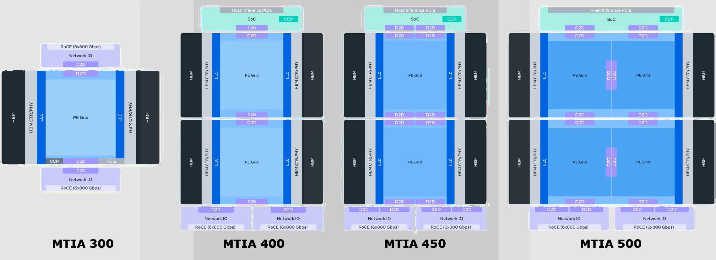 Meta's four-chip MTIA roadmap spans MTIA 300 through 500, with deployment every six months through 2027.
Source: xpu.pub / Meta
Meta's four-chip MTIA roadmap spans MTIA 300 through 500, with deployment every six months through 2027.
Source: xpu.pub / Meta
Performance Benchmarks
Every performance number for MTIA 400 comes from Meta. There are no independent benchmarks, no MLPerf submissions, no third-party testing. This is not unusual for internal silicon programs - AWS Trainium2 similarly withholds raw FLOPS, TDP, and process node details - but it does mean you're reading marketing material dressed up as technical specs.
Meta claims MTIA 400 is "competitive with leading commercial products." In early 2026, the realistic reference point for that phrase is the H100/MI300X generation - chips that were already being displaced by NVIDIA B200 and AMD MI350X by the time the MTIA 400 announcement dropped. For context:
| Metric | Meta MTIA 400 | NVIDIA H100 SXM5 | AMD MI300X |
|---|---|---|---|
| Peak FP8 TFLOPS | 6,000 | 3,958 | 2,610 |
| HBM Capacity | 288 GB | 80 GB | 192 GB |
| HBM Bandwidth | 9.2 TB/s | 3.35 TB/s | 5.3 TB/s |
| TDP | 1,200W | 700W | 750W |
| External Availability | None | Yes | Yes |
| Independent Benchmarks | None | Many | Many |
Raw FLOPS favor MTIA 400 on this comparison, but the numbers need context. First, 6 PFLOPS at 1,200W versus 3.9 PFLOPS at 700W means MTIA 400 delivers roughly 5 TFLOPS per watt versus H100's 5.6 TFLOPS per watt - not a power efficiency win. Second, the H100 and MI300X are mature products with years of compiler, driver, and software stack optimization. MTIA 400 runs on Meta's internal software stack tuned for Meta's specific model architectures. Real-world throughput on production GenAI workloads may or may not reflect the headline numbers. Meta hasn't said.
The MX4 figure - 12 PFLOPS - looks strong against anything in the H100/MI300X generation. But MX4 is a non-standard format that isn't supported by most training frameworks or model weights. Comparing it to FP8 TFLOPS from other vendors inflates the apparent lead.
Key Capabilities
Dual-Chiplet Compute Architecture. The MTIA 400 doubles the compute chiplets of the MTIA 300 - two compute dies versus one, plus dedicated network chiplets and HBM stacks in a multi-chip module. The network chiplets handle the PCIe host interface and networking functions independently of the compute dies, keeping collective communication traffic off the main compute path. This separation is architecturally clean: on GPU systems, NVLink and PCIe traffic competes with compute kernels for scheduling and memory resources. MTIA 400 avoids that by design. The RISC-V vector architecture from MTIA 300 carries through, with each Processing Element pairing RISC-V cores with a Dot Product Engine for dense matrix operations and a Special Function Unit for non-linear activations.
MX8 and MX4 Precision Support. MTIA 400 is the first MTIA chip to support Microscaling formats. MX8 and MX4 use block-level shared exponents - rather than each value carrying its own exponent, a block of values shares one exponent element encoded in higher precision. This compresses the bit budget per value while reducing the quantization error that comes from naively cutting exponent bits. The MX specification was co-developed by Microsoft, NVIDIA, AMD, Intel, Qualcomm, and Meta, and ratified through Open Compute Project, so it's an actual open standard rather than a proprietary Meta format. The practical upside is higher arithmetic throughput per watt at equivalent model quality for inference workloads - if Meta's software stack can actually exploit the format efficiently across its GenAI model mix. That's a meaningful if.
72-Chip Scale-Up Domain. A single rack of 72 MTIA 400 chips forms one scale-up domain through a switched backplane, with 1.2 Tbps of scale-up bandwidth across the domain. For reference, Google TPU v7 Ironwood targets pods of 9,216 chips. The MTIA 400 rack is a much smaller collective - appropriate for inference, where jobs are usually smaller than large training runs, but limited compared to what hyperscaler TPU programs can address. Scale-out networking runs at 100 Gbps, which handles communication between racks without the complexity of the scale-up backplane.
Expanded GenAI Workload Support. MTIA 300 focused on ranking and recommendation. MTIA 400 adds GenAI inference - image generation, video generation, and text generation across Meta's product surface. This is a significant expansion in workload complexity. R&R inference involves sparse embedding lookups and shallow models; GenAI inference involves large transformer models, long context handling, and KV cache management. Whether the MTIA 400 architecture handles both efficiently or simply handles both adequately is something Meta hasn't quantified externally.
Pricing and Availability
MTIA 400 isn't for sale. It won't be. No pricing exists because no transaction is possible. The chip is being rolled out in Meta's own data centers, serving Meta's own products, using Meta's own software stack. The Broadcom co-development partnership handles physical design and manufacturing coordination with TSMC; Broadcom doesn't get a commercial product out of this arrangement either.
If you need a custom inference ASIC, your options are AWS Trainium2 through EC2 instances, Google TPU v7 Ironwood through Google Cloud, or commercial hardware from NVIDIA, AMD, and others. MTIA 400 isn't and won't be on that list.
The strategic logic for Meta is straightforward. Meta's inference volume across Facebook, Instagram, WhatsApp, and AI products is enormous enough that custom silicon economics work even with the full R&D amortization. The chip doesn't have to be better than a H100 in every dimension - it just has to be better than a H100 for Meta's specific workloads at Meta's specific scale. Whether it hits that's something only Meta can verify.
Strengths and Weaknesses
Strengths
- HBM capacity (288 GB) and bandwidth (9.2 TB/s) exceed the H100 SXM5 substantially
- Dual-chiplet compute architecture doubles compute density versus MTIA 300
- MX4/MX8 support aligns with an open industry standard (Open Compute Project MX spec)
- 72-chip scale-up domain via switched backplane avoids PCIe bandwidth bottlenecks
- Part of a coherent four-generation roadmap with defined delivery targets
- Real deployment at Meta's scale, not a paper chip or lab demonstration
Weaknesses
- No external availability - zero relevance to anyone outside Meta
- All performance claims are self-reported; no independent verification is possible
- 6 PFLOPS at 1,200W isn't notably power efficient compared to H100's 3.9 PFLOPS at 700W
- MX4 PFLOPS number isn't comparable to FP8 PFLOPS from NVIDIA or AMD
- "Competitive with leading commercial products" is a vague claim probably indexed to H100 generation
- Process node undisclosed, preventing efficiency analysis
- Software stack is proprietary and non-transferable - no community, no open tooling
Related Coverage
- Meta MTIA 300 - the predecessor chip, 1.2 PFLOPS FP8, focused on ranking and recommendation
- Meta Unveils Four MTIA Chip Generations - the March 2026 roadmap announcement
- AWS Trainium2 - Amazon's internal-only training chip; same "hyperscaler custom silicon" category
- Google TPU v7 Ironwood - Google's inference-optimized TPU, also cloud-only
Sources
- Meta AI Blog: Four MTIA Chips in Two Years - Scaling AI Experiences for Billions (March 2026)
- Meta About Blog: Expanding Meta's Custom Silicon to Power Our AI Workloads (March 2026)
- Meta About Blog: Meta Partners With Broadcom to Co-Develop Custom AI Silicon (April 2026)
All MTIA 400 performance specifications - FP8 PFLOPS, MX4 PFLOPS, HBM capacity, HBM bandwidth, TDP, networking speeds, and scale-up domain size - are sourced from Meta's March 2026 technical announcement. No independent validation of these figures has been published.
✓ Last verified May 15, 2026
