Meta MTIA 300
Meta's first mass-deployed RISC-V AI accelerator - 1.2 PFLOPS FP8, 216 GB HBM, powering Facebook and Instagram at scale.

Overview
Meta's MTIA 300 is the chip actually running Facebook and Instagram right now. Not a research demo, not a paper - a production ASIC handling hundreds of thousands of ranking and recommendation inference requests per second across Meta's global infrastructure. The chip uses a RISC-V vector architecture co-developed with Broadcom and fabricated at TSMC, on a process node Meta hasn't disclosed. At 1.2 PFLOPS FP8 and 6.1 TB/s of HBM bandwidth in a 216 GB HBM package, MTIA 300 is a meaningful piece of silicon. But the more interesting story is what comes after it - Meta published a four-generation roadmap through 2027 that promises 25x the compute of MTIA 300 by the time MTIA 500 ships. Whether any of it can truly challenge NVIDIA at scale is a harder question than Meta's marketing suggests.
TL;DR
- RISC-V based ASIC co-developed with Broadcom, fabricated at TSMC (process node undisclosed)
- 1.2 PFLOPS FP8 compute, 6.1 TB/s HBM bandwidth, 216 GB HBM capacity
- 800W TDP - substantially lower than the H100's 700W only when you account for the gap in raw FLOPS
- Designed for ranking and recommendation training, not general-purpose LLM inference
- In production at Meta as of March 2026 - this is real deployment, not a lab chip
- Three successors planned through 2027 with 25x total compute scaling from 300 to 500
- Not available for purchase - internal use only
The architecture is more complex than a typical GPU-style accelerator. Each MTIA 300 chiplet assembly consists of one compute chiplet, two network chiplets, and HBM stacks. The compute chiplet contains a range of Processing Elements (PEs), each equipped with two RISC-V vector cores, a Dot Product Engine for matrix math, a Special Function Unit for non-linear activations, a Reduction Engine for collective operations, and a DMA engine for memory movement. The network chiplets handle off-chip communication through dedicated message engines - keeping collective communication traffic off the main compute path rather than mixing it with tensor operations the way standard GPU NVLink implementations do.
The RISC-V choice is unconventional for AI accelerators. Most custom silicon in this space - from Google's TPU to AWS Trainium - uses proprietary scalar or vector ISAs for their control cores, or custom VLIW processors. Meta went with an open standard. The practical benefit is toolchain maturity and the ability to reuse existing RISC-V compiler infrastructure rather than building a custom compiler from scratch. Whether this actually reduces development cost or just shifts where the complexity lives isn't something Meta has quantified publicly.
Broadcom's role as co-developer is significant. Meta doesn't design chips in-house the way Apple or Google do - the Broadcom partnership handles the physical design, packaging, and manufacturing coordination with TSMC. This is a similar model to what several hyperscalers use for their custom silicon programs, and it makes MTIA less of a pure in-house chip than the press coverage implies.
 Meta's MTIA roadmap covers four chip generations with deployments every six months through 2027.
Source: about.fb.com
Meta's MTIA roadmap covers four chip generations with deployments every six months through 2027.
Source: about.fb.com
Key Specifications
| Specification | Details |
|---|---|
| Manufacturer | Meta Platforms |
| Co-developer | Broadcom |
| Fabrication | TSMC (process node not disclosed) |
| Product Family | MTIA (Meta Training and Inference Accelerator) |
| Chip Type | ASIC |
| Architecture | RISC-V based; 1 compute chiplet + 2 network chiplets + HBM stacks |
| Processing Element | 2 RISC-V vector cores + DPE + SFU + Reduction Engine + DMA engine |
| Memory | 216 GB HBM |
| Memory Bandwidth | 6.1 TB/s |
| FP8 Performance | 1.2 PFLOPS (1,200 TFLOPS) |
| TDP | 800W |
| Primary Workload | Ranking and Recommendation (R&R) training |
| Status | In production (March 2026) |
| Availability | Internal use only - not sold commercially |
MTIA Roadmap
This chip doesn't make sense in isolation. Meta explicitly positioned the MTIA 300 launch as the foundation of a four-generation roadmap. Here's what the full path looks like:
| Chip | Status | FP8/MX4 FLOPS | HBM Bandwidth | HBM Capacity | TDP |
|---|---|---|---|---|---|
| MTIA 300 | In production | 1.2 PFLOPS | 6.1 TB/s | 216 GB | 800W |
| MTIA 400 | Lab testing, launches 2026 | ~6 PFLOPS | ~9.2 TB/s | ~288 GB | ~1,200W (est.) |
| MTIA 450 | Mass deploy early 2027 | ~21 PFLOPS | ~18.4 TB/s | ~288 GB | ~1,400W (est.) |
| MTIA 500 | Mass deploy 2027 | ~30 PFLOPS | ~27.6 TB/s | ~384-512 GB | ~1,700W (est.) |
The 300-to-500 headline numbers: 4.5x HBM bandwidth increase, 25x compute increase. Those are aggressive scaling targets. MTIA 400, currently in lab testing, doubles the compute chiplets and adds a 72-accelerator rack scale-up configuration with a switched backplane. It claims to be "competitive with leading commercial products" at launch - which presumably means the H100 generation, not Blackwell. MTIA 450 targets "much higher than leading commercial products" for MX4 FLOPS, which is a bolder claim that depends heavily on what the competition looks like in early 2027.
The compute format shift matters here. MTIA 300 uses FP8 precision. MTIA 400 shifts to MX8 (Microscaling 8-bit), and MTIA 450 and 500 use MX4 (Microscaling 4-bit). MX formats use block-level shared exponents to pack more precision into lower bit-width representations. The jump from 1.2 PFLOPS FP8 to 6 PFLOPS MX8 on MTIA 400 isn't just raw hardware scaling - it's partly a precision format change that inflates the FLOPS number in ways that aren't directly comparable to the MTIA 300 FP8 figure. Meta should be more explicit about this in its roadmap communications, and reviewers should treat the cross-generation FLOPS comparisons with appropriate skepticism.
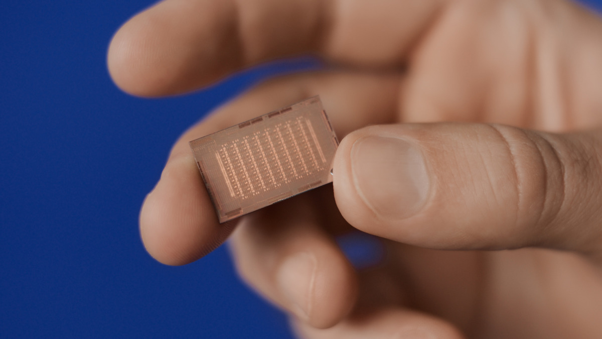 The MTIA chip package showing compute chiplet, network chiplets, and HBM stacks.
Source: ai.meta.com
The MTIA chip package showing compute chiplet, network chiplets, and HBM stacks.
Source: ai.meta.com
Performance Context
Comparing MTIA 300 to NVIDIA's current lineup requires care, because they target different workloads. The H100 SXM5 delivers 3,958 TFLOPS FP8 at 700W. The MTIA 300 delivers 1,200 TFLOPS FP8 at 800W. On raw FLOPS per watt, MTIA 300 is worse by a factor of roughly 3.7x. This isn't a competitive AI accelerator for general-purpose LLM training or inference.
Where MTIA 300 makes sense is ranking and recommendation (R&R) workloads. R&R inference is architecturally different from LLM inference - it involves sparse embedding table lookups, fairly shallow models, and batch patterns that don't play to GPU strengths. Meta has spent years improving its software stack for exactly these workloads on MTIA. The claim that MTIA delivers better cost efficiency than GPUs on R&R is plausible and probably true, but Meta hasn't published independent verification. Given that Meta has also signed multibillion-dollar deals with NVIDIA and AMD in the same period, it's clear that MTIA doesn't - and doesn't claim to - replace GPU infrastructure completely.
The MTIA 300 also can't be assessed like a chip you can buy and benchmark yourself. Every performance number comes from Meta, running Meta's workloads, on Meta's infrastructure. There's no MLPerf submission, no independent third-party testing. The 1.2 PFLOPS FP8 peak number is theoretical, and the real-world use rate on production R&R workloads isn't disclosed.
Key Capabilities
RISC-V Vector Architecture. Each Processing Element pairs two RISC-V vector cores with a dedicated Dot Product Engine. The vector cores handle general computation and control flow, while the DPE handles the dense matrix multiplications that dominate neural network layers. This division lets Meta tune the DPE specifically for the precision formats and matrix sizes that appear in R&R models without forcing the RISC-V cores to handle operations they aren't efficient at. The Reduction Engine enables collective operations like all-reduce within the PE array, which matters for training where gradient accumulation across many parallel compute units is a dominant cost.
Network Chiplet Architecture. The two dedicated network chiplets handle inter-chip communication independently of the compute chiplet. This separation is architecturally sound - on GPU clusters, NVLink and PCIe bandwidth compete with compute kernels for memory and scheduling resources. By moving all network traffic to dedicated silicon, Meta ensures that collective communications don't starve the main compute path. The network chiplets implement message engines that handle the protocol stack in hardware, reducing the CPU involvement required to coordinate large multi-chip training runs.
HBM Configuration. 216 GB of HBM is a large capacity - more than the H100 SXM5's 80 GB and comparable to H200's 141 GB, though less than some HBM3e configurations. The 6.1 TB/s bandwidth is the more interesting number: it's nearly double the H100's 3.35 TB/s. For R&R workloads that are memory-bandwidth-bound rather than compute-bound - large embedding tables require reading many parameters per inference request - high bandwidth relative to capacity is the right trade-off.
Multi-Generation Software Stack. Meta has been running MTIA in production since at least 2023 with earlier generations. The MTIA 300 benefits from a maturing software stack tuned for Meta's specific workload mix. This is where custom silicon programs have advantages that raw FLOPS comparisons miss - years of compiler optimization, operator fusion, and model-hardware co-design that a general-purpose GPU can't match for a specific workload category.
Pricing and Availability
MTIA 300 isn't available for purchase. It's internal-only silicon, designed and rolled out exclusively in Meta's own data centers. There is no pricing, no cloud API offering, no hardware sales program. If you want to run workloads on MTIA, the answer is: you can't.
This makes MTIA a poor comparison point for organizations evaluating AI accelerator options. The relevant question for Meta is whether MTIA delivers better cost efficiency than the H100 and MI300X they'd otherwise buy, not whether it's competitive as a product. Meta spending its own R&D budget on chips that only it can use is a bet that the volume of AI infrastructure it needs is large enough to amortize the development cost.
Given Meta's scale - hundreds of thousands of inference requests per second across Facebook, Instagram, and WhatsApp - that bet is probably correct. The R&D cost of MTIA is spread across an enormous production workload. For any other company, the math wouldn't work.
Strengths and Weaknesses
Strengths:
- Proven in production at massive scale - this isn't a paper chip
- High HBM bandwidth (6.1 TB/s) suited to memory-bandwidth-bound R&R workloads
- Dedicated network chiplets separate communication from compute
- RISC-V foundation gives access to mature open toolchains
- Aggressive roadmap with clear targets through 2027
Weaknesses:
- Not available for any external use - zero practical relevance outside Meta
- 1.2 PFLOPS FP8 isn't competitive with NVIDIA H100 (3.9 PFLOPS) or AMD MI300X (2.6 PFLOPS)
- No independent performance benchmarks - all numbers are Meta self-reported
- Process node undisclosed, making power efficiency comparisons difficult
- RISC-V at the PE level hasn't been proven at scale for LLM training (which MTIA 400 targets)
- Precision format shift across generations (FP8 to MX8 to MX4) makes roadmap FLOPS comparisons unreliable
Related Coverage
- Meta Unveils Four MTIA Chip Generations in Two Years - Detailed roadmap breakdown
- Groq LPU - Deterministic Inference at Scale - Another custom inference ASIC taking a radically different approach
- AWS Trainium2 - Amazon's custom training silicon, also internal-use only
- Google TPU v7 Ironwood - Google's seventh-generation TPU
Sources
- Meta Engineering Blog: MTIA chip roadmap announcement (March 2026) - engineering.fb.com
- Meta AI Blog: First-generation MTIA experiences (2023) - ai.meta.com
- Meta About Blog: MTIA four-chip roadmap details - about.fb.com
Meta's March 2026 roadmap briefing confirmed MTIA 300 at 1.2 PFLOPS FP8, 6.1 TB/s bandwidth, and 216 GB HBM, with MTIA 400 currently in lab testing ahead of 2026 deployment.
✓ Last verified March 15, 2026

