Intel Gaudi 3 - Challenging NVIDIA on Price
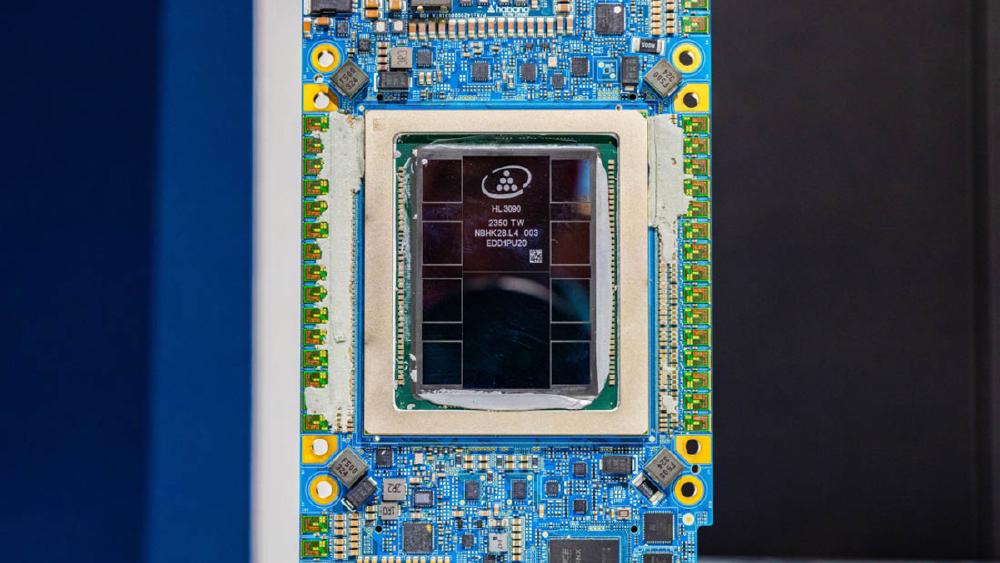
Intel Gaudi 3 is a TSMC 5nm AI accelerator with 128GB HBM2e and 1,835 TFLOPS FP8 performance, positioned as a cost-effective alternative to NVIDIA H100 for training and inference workloads.
TL;DR
- Third-generation AI accelerator from Intel (originally Habana Labs), fabricated on TSMC 5nm
- 128GB HBM2e with 3,700 GB/s bandwidth - 60% more memory capacity than NVIDIA H100's 80GB
- 1,835 TFLOPS FP8 performance across 64 Tensor Processor Cores and 8 Matrix Math Engines
- Estimated street price around $15,000 per accelerator - roughly 40-50% cheaper than H100 SXM
- Integrated 24x 200GbE RDMA networking eliminates the need for external NICs in training clusters
Overview
Intel Gaudi 3 is the company's most serious attempt to break NVIDIA's stranglehold on the AI accelerator market. Acquired through the $2 billion Habana Labs purchase in 2019, the Gaudi line has always been positioned on price - offering competitive performance at a significantly lower cost than NVIDIA equivalents. Gaudi 2 gained traction with cloud providers and enterprise buyers who were willing to trade some CUDA convenience for meaningful cost savings. Gaudi 3 raises the stakes by moving to TSMC 5nm, doubling the compute performance over Gaudi 2, and targeting direct competition with the NVIDIA H100 on both training and inference workloads.
The specs are respectable. 128GB of HBM2e provides 60% more memory capacity than an H100 SXM's 80GB, which means larger models can fit on a single card without resorting to multi-card tensor parallelism. The 3,700 GB/s of memory bandwidth is competitive with the H100's 3,350 GB/s HBM3 bandwidth. The 1,835 TFLOPS of FP8 compute trails the H100's 3,958 TFLOPS by about 54%, but at an estimated ~$15,000 per card versus ~$25,000-30,000 for an H100 SXM, the price-performance ratio tilts in Gaudi 3's favor for many workloads.
The real challenge for Gaudi 3 is not hardware - it is software. NVIDIA's CUDA ecosystem has had over 15 years to mature, and virtually every AI framework, library, and optimization toolkit is built around it. Intel's software stack - SynapseAI for Gaudi-specific operations and oneAPI for broader Intel hardware - is improving rapidly but remains a generation behind in tooling, documentation, and community support. For organizations willing to invest in the integration work, Gaudi 3 offers meaningful cost savings. For those who need to ship next quarter with minimal engineering risk, the CUDA ecosystem is still the path of least resistance.
Key Specifications
| Specification | Details |
|---|---|
| Manufacturer | Intel (Habana Labs) |
| Product Family | Gaudi (3rd generation) |
| Chip Type | ASIC |
| Process Node | TSMC 5nm |
| Tensor Processor Cores (TPCs) | 64 |
| Matrix Math Engines (MMEs) | 8 |
| On-Chip SRAM | 48MB |
| HBM Memory | 128GB HBM2e (8 stacks) |
| Memory Bandwidth | 3,700 GB/s |
| FP8 Performance | 1,835 TFLOPS |
| BF16 Performance | 1,835 TFLOPS |
| TF32 Performance | ~460 TFLOPS (estimated) |
| FP32 Performance | ~460 TFLOPS (estimated) |
| TDP | 900W |
| RDMA Networking | 24x 200GbE (integrated on-die) |
| Aggregate Network Bandwidth | 4.8 Tbps |
| Host Interface | PCIe Gen5 x16 |
| Form Factors | HL-325L (OAM), HL-388 (PCIe) |
| Target Workload | Training and Inference |
| Estimated Price | ~$15,000 per accelerator |
| Release | Q3 2024 |
Performance Benchmarks
| Metric | Intel Gaudi 3 | NVIDIA H100 (SXM) | NVIDIA A100 (80GB) | AMD MI300X |
|---|---|---|---|---|
| FP8 TFLOPS | 1,835 | 3,958 | N/A (no FP8) | 2,615 |
| BF16 TFLOPS | 1,835 | 1,979 | 312 | 1,308 |
| HBM Capacity | 128GB | 80GB | 80GB | 192GB |
| HBM Bandwidth | 3,700 GB/s | 3,350 GB/s | 2,039 GB/s | 5,300 GB/s |
| TDP | 900W | 700W | 400W | 750W |
| RDMA Networking | 24x 200GbE (on-die) | NVLink + external IB | NVLink + external IB | IF + external |
| Estimated Card Price | ~$15K | ~$25-30K | ~$10-15K | ~$15-20K |
| LLM Training (vs H100) | ~0.6-0.75x | 1.0x (baseline) | ~0.35x | ~0.7-0.85x |
| LLM Inference (vs H100) | ~0.65-0.8x | 1.0x (baseline) | ~0.3x | ~0.8-0.9x |
On raw FP8 FLOPS, Gaudi 3 is about 46% of an H100. But the picture shifts when you factor in price. At ~$15K versus ~$25-30K, Gaudi 3 delivers roughly 80-90% of the FP8 TFLOPS per dollar. The BF16 numbers are even more competitive - 1,835 TFLOPS at $15K versus 1,979 TFLOPS at $25-30K means Gaudi 3 is actually better on BF16 price-performance than the H100.
Intel claims that for specific workloads - particularly large-scale LLM training with models like Llama 2 70B - Gaudi 3 achieves within 15-25% of H100 performance at roughly half the price. Independent benchmarks have generally confirmed savings in the 30-50% range for well-supported model architectures, though the gap with H100 widens on heavily optimized CUDA workloads where NVIDIA's kernel libraries (cuBLAS, cuDNN, FlashAttention) have years of hand-tuned optimization.
Memory Capacity Advantage
The 128GB HBM2e is an underappreciated advantage. For large language model inference, the ability to fit a complete model on a single card eliminates multi-card tensor parallelism overhead.
A 70B parameter model in FP8 precision requires about 70GB - well within Gaudi 3's 128GB but dangerously close to the H100's 80GB limit after accounting for KV cache and activation memory.
At FP16 precision, a 70B model requires 140GB, which exceeds the H100's capacity entirely but fits on two Gaudi 3 cards rather than three H100 cards.
For inference workloads with large KV caches - long-context models, multi-turn conversations, or RAG pipelines that maintain large context windows - the extra 48GB of HBM capacity on Gaudi 3 can be the difference between serving a model on one card versus two. That is a 50% reduction in hardware cost per inference instance.
To put it concretely: if you are serving a 70B model with a 32K token context window, the KV cache alone can consume 20-40GB depending on the attention architecture. On an H100 with 80GB total, fitting the 70GB model weights plus a 30GB KV cache is impossible. On Gaudi 3 with 128GB, it fits with headroom to spare.
The Integrated Networking Advantage
The integrated networking deserves special attention because it fundamentally changes the system economics for multi-node training clusters.
Gaudi 3 includes 24 ports of 200Gbps Ethernet RDMA directly on the accelerator die, providing 4.8 Tbps of aggregate networking bandwidth per chip without requiring a single external network interface card.
For comparison, an NVIDIA H100 DGX system requires separate ConnectX-7 InfiniBand adapters (typically 8x 400Gbps) for inter-node communication, in addition to the NVLink interconnect for intra-node GPU-to-GPU communication. These NICs add $3,000-5,000 per adapter to the system cost, and the InfiniBand switches and cabling add further infrastructure expense.
In a 128-node training cluster, the networking infrastructure can represent 15-25% of total system cost. Gaudi 3 eliminates this entire cost layer. The RDMA networking is on the die - no external NICs, no NIC-to-chip PCIe bottleneck, no additional power draw for networking hardware.
Intel estimates that integrated networking reduces total system cost by 10-20% compared to equivalent GPU clusters, with the savings scaling proportionally with cluster size. For a 256-card deployment, this can translate to hundreds of thousands of dollars in saved infrastructure costs.
The integrated networking also simplifies system design. Each Gaudi 3 card appears as a network endpoint on the Ethernet fabric. There is no need to configure NVLink topologies, map NUMA domains to NICs, or optimize PCIe lane assignments for network traffic. Standard Ethernet switches and cables handle the inter-node communication, reducing the need for specialized networking expertise.
Key Capabilities
Dual Compute Architecture - TPCs and MMEs. Gaudi 3's compute architecture splits work between two types of processing units: 64 Tensor Processor Cores (TPCs) and 8 Matrix Math Engines (MMEs).
The MMEs handle dense matrix multiplications - the core operation in transformer attention and feed-forward layers. These are fixed-function engines optimized for high-throughput matrix operations at FP8, BF16, and FP32 precision.
The TPCs handle everything else: activation functions, normalization layers, element-wise operations, custom kernels, and any computation that does not fit the matrix multiplication pattern. TPCs are fully programmable using TPC-C, a C-like language that gives developers control over the compute pipeline.
This dual architecture allows Gaudi 3 to overlap matrix computation on the MMEs with non-matrix operations on the TPCs, improving utilization compared to GPU architectures where the same streaming multiprocessors handle both types of work.
Intel claims this dual-compute approach delivers higher sustained utilization on real training workloads compared to GPU architectures that must context-switch between matrix and non-matrix operations on the same hardware. The separation simplifies the compiler's scheduling problem - MMEs run a predictable dataflow pattern while TPCs handle the irregular computation that would otherwise create pipeline bubbles.
SynapseAI Software Stack. Intel's SynapseAI SDK is the bridge between Gaudi 3 hardware and standard AI frameworks. The stack includes:
- Graph compiler: Optimizes computation graphs for Gaudi's TPC and MME architecture, handling operator fusion, memory management, and data layout optimization automatically
- Model Reference Library: Pre-optimized implementations for common architectures including GPT, Llama 2/3, Stable Diffusion, Mixtral, BERT, ViT, and Whisper
- Profiler: Performance debugging tools for identifying bottlenecks in custom models
- PyTorch bridge: Integration via the
habana_frameworkspackage, replacing CUDA device calls with HPU device calls - DeepSpeed integration: Support for ZeRO optimization stages and pipeline parallelism through DeepSpeed for Habana
For models already in the SynapseAI Model Reference library, the porting effort from CUDA is minimal. The typical migration involves:
- Changing the device target from
cudatohpu - Replacing CUDA-specific data loaders with Habana-optimized versions
- Adjusting distributed training configuration for Gaudi's networking topology
- Running the SynapseAI graph compiler to optimize the computation graph
Intel has invested heavily in making this migration path as smooth as possible, including compatibility layers for common PyTorch patterns. For well-supported models, the entire process can be completed in a few days.
For custom models with novel operators not in the SynapseAI library, the porting effort scales significantly. Each custom CUDA kernel must be reimplemented using TPC-C or the SynapseAI high-level API. A custom FlashAttention variant that took one engineer a week to optimize on CUDA might take two to four weeks to port and optimize for Gaudi.
This is the primary friction point for adoption, and it is where the CUDA ecosystem advantage is most acute. The SynapseAI documentation is good but not comprehensive. Community examples are sparse. Stack Overflow threads about Gaudi optimization are rare. The developer experience gap with CUDA is real and should not be underestimated.
Flexible Precision Support. Gaudi 3 supports FP8 (E4M3 and E5M2), BF16, FP16, FP32, and TF32 data types. A notable property of Gaudi 3's architecture is that the FP8 and BF16 performance are identical at 1,835 TFLOPS.
On NVIDIA's H100, FP8 delivers 3,958 TFLOPS while BF16 delivers 1,979 TFLOPS - a 2x difference. This means H100 users face a strong incentive to use FP8 for maximum throughput, even when BF16 would produce better training results.
Gaudi 3 users who want higher precision training (BF16 instead of FP8) pay zero performance penalty in terms of peak FLOPS. For workloads where FP8 precision is insufficient - certain scientific computing tasks, fine-tuning scenarios where precision matters, or applications where BF16 is the established standard - Gaudi 3's flat precision curve is a genuine advantage.
The practical implication is that Gaudi 3's BF16 performance (1,835 TFLOPS at ~$15K) is directly competitive with the H100's BF16 performance (1,979 TFLOPS at ~$25-30K). On a BF16 price-performance basis, Gaudi 3 is roughly 70-80% cheaper per TFLOPS than the H100.
This matters more than it might seem. Many production training runs still use BF16 rather than FP8, either because the model architecture has not been validated with FP8 precision or because the application requires the higher fidelity of BF16 gradients. For these workloads, Gaudi 3 offers a compelling cost advantage.
Pricing and Availability
Intel has not published an official MSRP for Gaudi 3, but industry estimates place the per-accelerator price at approximately $15,000 - roughly 40-50% less than an NVIDIA H100 SXM.
The Gaudi 3 accelerator is available in two form factors:
- HL-325L: OAM (OCP Accelerator Module) form factor for server integration
- HL-388: PCIe card form factor for more flexible deployment
| Accelerator | Est. Price | FP8 TFLOPS | $/FP8 TFLOPS | BF16 TFLOPS | $/BF16 TFLOPS |
|---|---|---|---|---|---|
| Intel Gaudi 3 | ~$15,000 | 1,835 | ~$8.17 | 1,835 | ~$8.17 |
| NVIDIA H100 SXM | ~$27,500 | 3,958 | ~$6.95 | 1,979 | ~$13.90 |
| NVIDIA A100 80GB | ~$12,500 | N/A | N/A | 312 | ~$40.06 |
| AMD MI300X | ~$17,500 | 2,615 | ~$6.69 | 1,308 | ~$13.38 |
On FP8 price-per-TFLOPS, Gaudi 3 is slightly more expensive than H100 and MI300X. But the BF16 column tells a different story - Gaudi 3 is roughly 40% cheaper per BF16 TFLOPS than both the H100 and MI300X.
Cluster Economics
The total system cost advantage comes at the cluster level. Consider a 64-card training cluster:
Gaudi 3 cluster:
- 64 x $15K (accelerator cards) = $960K
- Server chassis and networking = ~$240-540K (Ethernet switches, standard cabling)
- Total: ~$1.2-1.5M
H100 cluster:
- 64 x $27.5K (accelerator cards) = $1.76M
- 64 x $4K (ConnectX-7 NICs) = $256K
- InfiniBand switches and cabling = ~$400-700K
- Server chassis = ~$200-400K
- Total: ~$2.6-3.1M
That is roughly a 2x difference in total cluster cost. Even accounting for the H100's higher per-card performance, the Gaudi 3 cluster delivers competitive training throughput per dollar for well-supported model architectures.
Cloud Availability
Cloud availability has been expanding. Gaudi 3 instances are available on:
- Intel Developer Cloud: Direct access through Intel's cloud platform
- Select cloud partners: Various regional and specialty cloud providers
However, availability remains significantly more limited than NVIDIA GPU instances, which are offered by every major cloud provider globally with spot, reserved, and on-demand pricing tiers. Spot pricing and reserved instance discounts for Gaudi 3 are not yet widely available.
For organizations evaluating Gaudi 3, the limited cloud availability means that testing and prototyping can be more difficult than with NVIDIA GPUs, which can be spun up on AWS, GCP, Azure, or dozens of smaller providers within minutes.
The Habana Labs Story
Understanding Gaudi 3's position in the market requires understanding its origin. Habana Labs was founded in 2016 in Israel with the explicit goal of building AI training accelerators that could compete with NVIDIA on price. The company launched Gaudi 1 in 2019 - the same year Intel acquired it for $2 billion.
Under Intel's ownership, Habana Labs has operated as a semi-independent unit, maintaining its chip design team in Israel while leveraging Intel's manufacturing and go-to-market resources. Gaudi 2 was the first major post-acquisition product, gaining traction with AWS (which offered it as DL1 instances) and several enterprise customers.
Gaudi 3 represents the maturation of this strategy. The move from Intel's own process nodes to TSMC 5nm was a pragmatic decision - TSMC's 5nm delivers better density and power efficiency than Intel's equivalent nodes at the time of design. It also aligns Gaudi 3's manufacturing with the same foundry used by NVIDIA (H100 is TSMC 4nm) and AMD (MI300X is TSMC 5nm/6nm), putting the chips on comparable silicon footing.
The strategic question is whether Intel will sustain investment in the Gaudi line. Intel has reorganized its AI hardware strategy multiple times, and the cancellation of Falcon Shores (which was meant to merge Gaudi and Xe GPU architectures) raised questions about the long-term roadmap. Gaudi 3 is shipping and performing well, but buyers making 3-5 year infrastructure commitments should factor in Intel's historically variable commitment to non-CPU product lines.
Who Should Consider Gaudi 3
Strong fit:
- Organizations building 64+ card training clusters where system-level TCO matters
- Teams that primarily train well-supported model architectures (Llama, GPT, Stable Diffusion)
- Workloads that require BF16 precision where Gaudi 3's flat precision curve is an advantage
- Cost-sensitive deployments that can tolerate the engineering investment to migrate from CUDA
- Inference workloads with large KV cache requirements that benefit from 128GB HBM capacity
Weak fit:
- Teams shipping on tight timelines that cannot absorb CUDA-to-SynapseAI migration effort
- Research labs running novel model architectures with custom CUDA kernels
- Organizations that need broad cloud availability and multi-provider flexibility
- Small-scale deployments (1-4 cards) where the networking advantage does not apply
- Workloads that depend on NVIDIA-specific optimizations (TensorRT, Triton kernels)
Strengths
- ~40-50% lower per-accelerator price than NVIDIA H100 SXM
- 128GB HBM2e provides 60% more memory capacity than H100 - fits larger models per card
- 3,700 GB/s memory bandwidth is competitive with H100 HBM3
- Integrated 24x 200GbE RDMA networking eliminates external NIC costs and complexity
- Equal BF16 and FP8 performance means no precision penalty for higher-quality training
- SynapseAI has pre-optimized implementations for major model architectures
- System-level TCO savings of 30-50% for large training clusters versus NVIDIA equivalents
Weaknesses
- Raw FP8 FLOPS trails H100 by 54% - purely compute-bound workloads will be significantly slower
- SynapseAI software ecosystem is meaningfully less mature than NVIDIA CUDA
- Limited cloud availability compared to ubiquitous H100 and A100 instances
- Custom model porting from CUDA can require weeks of engineering work per novel operator
- 900W TDP is the highest of any single accelerator on this list - power and cooling demands are high
- Intel's AI accelerator strategy has shifted multiple times - long-term roadmap confidence is lower
- Community support, tutorials, and third-party tooling lag far behind the NVIDIA ecosystem
Related Coverage
- Groq LPU - A pure inference ASIC with a radically different SRAM-based architecture
- Cerebras WSE-3 - Wafer-scale computing with 21 PB/s on-chip bandwidth for training and inference
- AWS Trainium2 - Another non-NVIDIA training chip, available exclusively through AWS cloud
Sources
