Google TPU 8i - Low-Latency Inference for Agent Era
Google's TPU 8i is a purpose-built inference chip with 10.1 FP4 PFLOPs, 288GB HBM3e at 8,601 GB/s, and a Boardfly topology that cuts collective latency 5x for agentic AI workloads.
TL;DR
- Google's eighth-generation inference chip: 10.1 FP4 PFLOPs and 288GB HBM3e at 8,601 GB/s
- 384MB on-chip SRAM - 3x the TPU v7 Ironwood - enables larger KV caches for long-context reasoning
- Boardfly topology reduces maximum network diameter by 56% vs standard 3D torus for lower all-to-all latency
- 80% better performance-per-dollar for inference vs previous generation; 5x lower collective operation latency
Overview
The Google TPU 8i is the inference half of Google's eighth-generation TPU program, announced at Google Cloud Next on April 22, 2026 with the training-focused TPU 8t. The separation of training and inference into two dedicated chips is new for the TPU line, and the 8i shows exactly what Google focused on when it could make inference-specific design choices: more on-chip memory, a topology built for low-latency collective operations, and host CPU integration that reduces orchestration overhead.
Per chip, the 8i delivers 10.1 FP4 petaFLOPS with 288GB of HBM3e running at 8,601 GB/s - more memory and more bandwidth per chip than the 8t's 6,528 GB/s, because inference is memory-bandwidth-bound in a way that training isn't. The 384MB of on-chip SRAM is especially significant: three times what the Ironwood carried, and enough to hold much larger KV caches in-SRAM during multi-step reasoning and agent chains.
At the pod level, 1,152 TPU 8i chips form a single system image delivering 11.6 FP8 ExaFLOPS. Google uses this configuration for what it calls the "agentic era" - not batch throughput maximization, but fast response times for multi-step agent workflows where latency compounds across each reasoning hop.
Key Specifications
| Specification | Details |
|---|---|
| Manufacturer | |
| Product Family | 8th Generation TPU |
| Chip Type | TPU (ASIC) |
| Process Node | TSMC N3 |
| Memory | 288GB HBM3e |
| Memory Bandwidth | 8,601 GB/s |
| FP4 Performance | 10.1 PFLOPs per chip |
| FP8 Performance | Not disclosed |
| On-Chip SRAM | 384 MB (3x previous gen) |
| TDP | Not disclosed |
| Inter-Chip Interconnect (ICI) | 19.2 Tb/s (2x vs prior gen) |
| Network Topology | Boardfly (high-radix, max 7 hops) |
| Collective Latency | 5x reduction vs prior topology |
| Pod Scale | 1,152 chips, 11.6 FP8 ExaFLOPS |
| Host CPU | Dual Axion ARM (NUMA per server) |
| Cooling | 4th-generation liquid cooling |
| Release Date | 2026-H2 |
Performance Benchmarks
Google positions the 8i as a 80% improvement in price-performance over the Ironwood TPU for inference at low-latency targets. The comparison points that matter most for inference are memory bandwidth, on-chip SRAM, and collective latency - not raw TFLOPS.
| Metric | Google TPU 8i | Google TPU v7 Ironwood | Groq LPU | Notes |
|---|---|---|---|---|
| FP4 TFLOPS per chip | 10,100 | Not disclosed | N/A | Ironwood specs not public |
| FP8 TFLOPS per chip | Not disclosed | Not disclosed | ~429,000 | Groq TFLOPS not directly comparable |
| HBM Capacity | 288 GB HBM3e | 192 GB (est.) | None (SRAM only) | |
| Memory Bandwidth | 8,601 GB/s | Not disclosed | ~80 TB/s | Groq uses SRAM, different regime |
| On-chip SRAM | 384 MB | ~128 MB (est.) | 230 MB | |
| Inference Price-Performance | 1.8x vs Ironwood | (baseline) | Competitive | Google stated 80% improvement |
| Network Latency | 5x lower (CAE) | (baseline) | Near-zero | Different architectures |
The Groq LPU comparison deserves a note: Groq's numbers aren't directly comparable because it uses SRAM rather than HBM, operates in a different throughput/latency tradeoff space, and serves different model size ranges. For very large models (100B+), the TPU 8i's 288GB HBM gives it a clear capacity advantage. For fast single-stream latency on smaller models, Groq remains the benchmark.
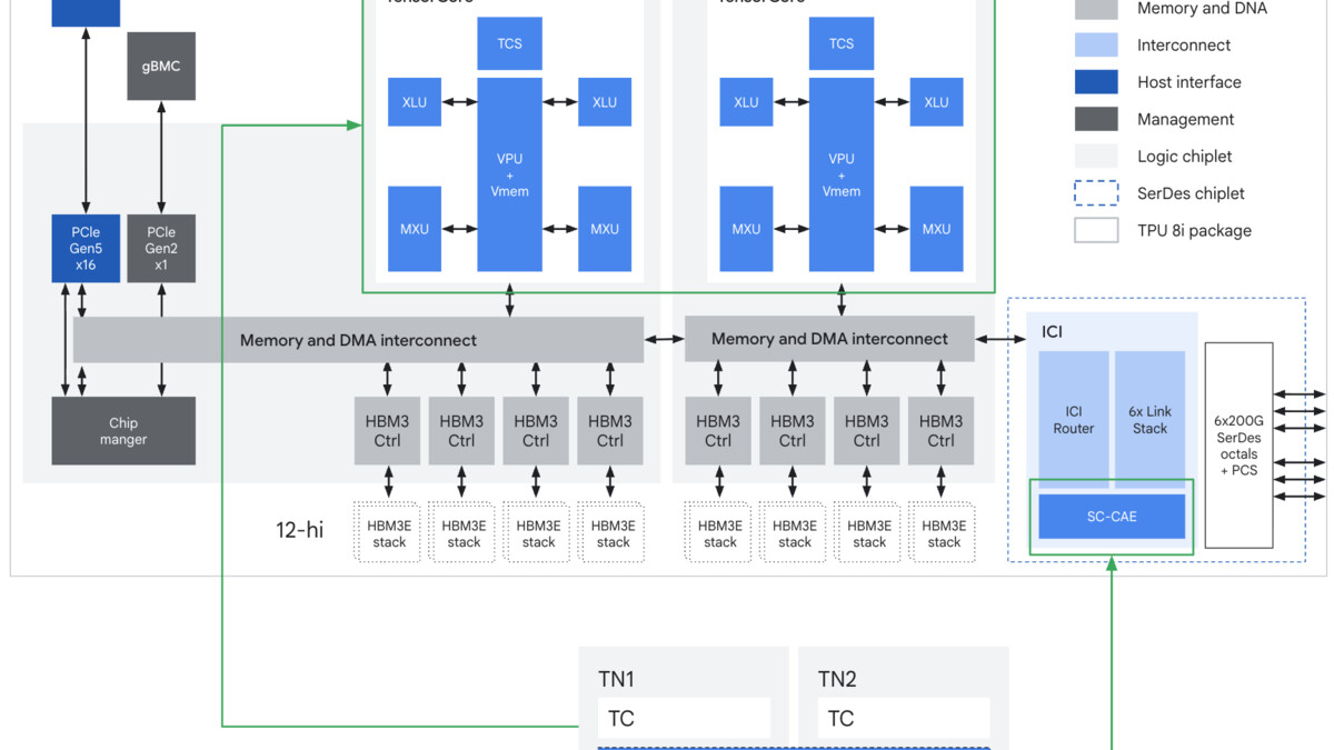 TPU 8i chip block diagram with Collectives Acceleration Engine (CAE), expanded SRAM, and HBM3e stacks.
Source: cloud.google.com
TPU 8i chip block diagram with Collectives Acceleration Engine (CAE), expanded SRAM, and HBM3e stacks.
Source: cloud.google.com
Key Capabilities
Boardfly Topology. The TPU 8i uses a different network topology than the 8t. Instead of a 3D torus (which the training chip uses for its different communication patterns), the 8i uses "Boardfly" - a high-radix topology that reduces the maximum number of hops between any two chips to seven. That's a 56% reduction in network diameter versus the previous generation's torus topology. For inference workloads, all-to-all communication (KV cache sharing across chips, attention head distribution, prefill/decode coordination) controls the communication profile. Fewer hops means lower latency at every step of an agentic chain.
Collectives Acceleration Engine. The CAE is an on-chip hardware block dedicated to collective operations - reduce, all-reduce, broadcast, scatter, gather. These are the communication primitives that inference serving frameworks use constantly to coordinate across chips. On the Ironwood, these operations ran on the main compute pipeline. On the 8i, they run on dedicated hardware with a claimed 5x reduction in collective operation latency. For a multi-step reasoning chain with dozens of communication rounds, this compounds clearly.
384MB SRAM and KV Cache. The three-fold increase in on-chip SRAM directly enables larger KV caches in-SRAM. KV cache is the memory that stores attention keys and values during autoregressive token generation - it grows with context length and number of concurrent requests. Keeping more of it in SRAM rather than HBM reduces the memory access latency for each token generation step. For long-context reasoning (64K+ tokens) or batch serving with many concurrent sessions, this matters.
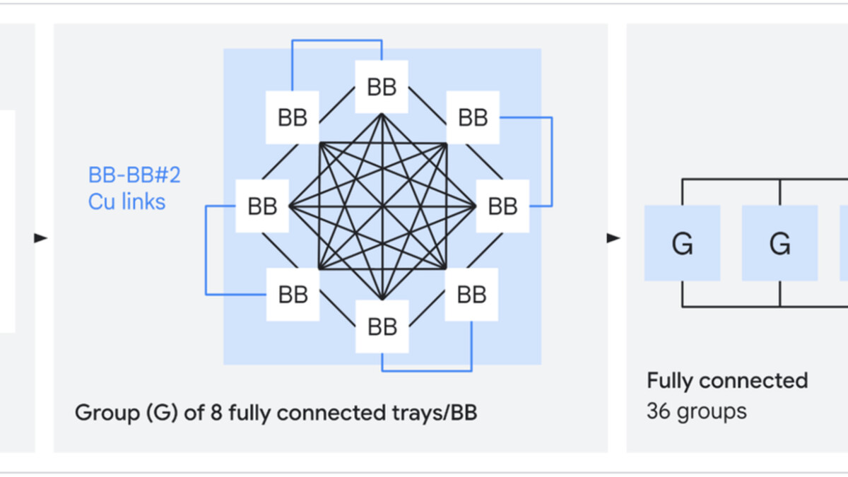 The Boardfly topology used by the TPU 8i, showing maximum seven-hop ICI network diameter.
Source: cloud.google.com
The Boardfly topology used by the TPU 8i, showing maximum seven-hop ICI network diameter.
Source: cloud.google.com
Pricing and Availability
No pricing has been published. The TPU 8i is a Google Cloud service and won't be available for on-premises deployment or through other cloud providers. Availability is scheduled for later in 2026.
For inference specifically, Google is competing against NVIDIA's inference offerings (including via the NVIDIA Groq 3 LPU partnership), Groq directly, and cloud providers reselling GPU capacity. The 80% price-performance improvement claim over Ironwood means little without an absolute price anchor - organizations assessing the 8i will need to wait for Google to publish per-chip-hour pricing before building a TCO model.
Strengths and Weaknesses
Strengths
- 288GB HBM3e at 8,601 GB/s per chip - more memory than AMD MI300X at higher bandwidth
- 384MB on-chip SRAM (3x Ironwood) enables much larger in-SRAM KV caches
- Boardfly topology: 56% reduction in max network diameter, 5x lower collective latency
- 80% better inference price-performance vs Ironwood
- Dual Axion ARM hosts per server for low-overhead orchestration
- Native support for vLLM, SGLang, JAX, and PyTorch - no custom framework required
Weaknesses
- Cloud-only: no on-premises deployment option
- FP8 TFLOPS not disclosed - limits direct comparison with GPU-based inference
- TDP not disclosed
- Training workloads require the separate TPU 8t
- Locked to Google Cloud availability schedule and pricing
Related Coverage
- Google TPU 8t - The companion training chip with superpod-scale architecture
- Google TPU v7 Ironwood - The predecessor inference chip
- Groq LPU - The primary alternative for ultra-low latency inference
- NVIDIA Groq 3 LPU - The NVIDIA-integrated LPU inference accelerator
Sources
✓ Last verified May 1, 2026
