Etched Sohu - Transformer-Only Inference ASIC
Full specs and critical analysis of the Etched Sohu - a transformer-specific ASIC claiming 500K+ tokens/sec on Llama 70B, built on TSMC 4nm with 144GB HBM3E. Bold claims, but no independent benchmarks yet.
TL;DR
- Transformer-specific ASIC on TSMC 4nm that hard-wires the transformer computation graph - attention, linear projections, softmax, and layer normalization are all baked into silicon
- Claims 500,000+ tokens per second on Llama 70B with a 8-chip server - versus ~23,000 tok/s on 8x H100 and ~45,000 tok/s on 8x B200
- 144GB HBM3E per chip on a reticle-limit die with claimed 90%+ FLOPS utilization
- $625M+ in total funding at a $5B+ valuation - but the chip hasn't shipped to customers and no independent benchmarks exist as of March 2026
- Can't run CNNs, LSTMs, SSMs (Mamba), or any non-transformer architecture - a deliberate and permanent trade-off
Overview
Etched is making the biggest bet in AI hardware: that the transformer architecture is permanent. Their Sohu chip hard-wires the entire transformer computation graph into silicon, removing the general-purpose programmability that makes GPUs flexible but inefficient. If transformers remain the dominant architecture for AI, Sohu could deliver an order-of-magnitude improvement in inference throughput per dollar. If the industry moves to a different architecture - state-space models, mixture-of-experts with non-attention routing, or something not yet invented - Sohu becomes an expensive paperweight.
Founded in 2022 by Gavin Uberti, Chris Zhu, and Robert Wachen (all Harvard dropouts), Etched announced Sohu in June 2024 with eye-catching claims: a 8-chip Sohu server creating over 500,000 tokens per second on Llama 70B, replacing 160 H100 GPUs. The company has since raised over $625 million in total funding at a reported $5 billion valuation, with backing from Primary Venture Partners, Lux Capital, and several prominent Silicon Valley investors.
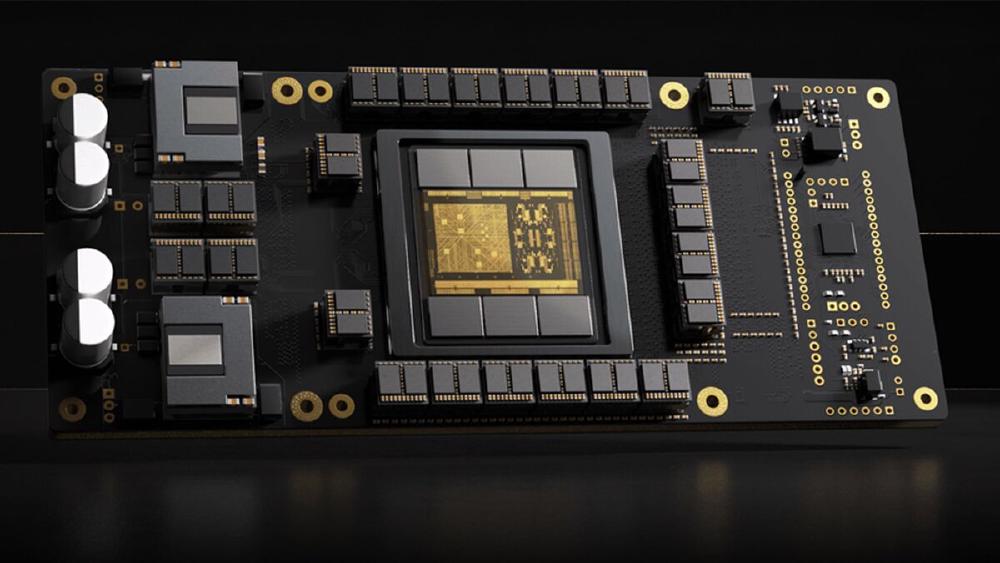
The chip is fabricated on TSMC's 4nm process at reticle-limit die size (the largest die that can be printed in a single lithographic exposure, roughly 800mm^2). It features 144GB of HBM3E memory. The architecture builds the transformer computation - multi-head attention with QKV projection, softmax, output projection, feed-forward network with GELU/SiLU activation, and layer normalization - as dedicated hardware blocks rather than programmable compute units. This means the chip doesn't execute instructions in the traditional sense; instead, data flows through a fixed pipeline of hardwired operations.
The claimed 90%+ FLOPS use is the key performance argument. On a general-purpose GPU like the H100, transformer inference typically hits 30-40% of peak FLOPS due to the overhead of instruction fetch/decode, memory management, thread scheduling, and kernel launch. By eliminating all of this overhead, Sohu can theoretically deliver 2-3x more useful compute from the same number of transistors. Etched claims the total speedup - including the benefits of specialization beyond just utilization - reaches 20x over the H100 for Llama 70B inference.
Here is where I need to be direct: none of these claims have been independently verified. As of March 2026, Sohu hasn't shipped to customers. No third-party benchmarks exist. No inference provider has published production throughput numbers. The 500,000 tok/s claim comes completely from Etched's own marketing materials and demo videos. For a chip with this much funding and this much hype, the absence of independent validation is the single most important fact to know.
Key Specifications
| Specification | Details |
|---|---|
| Manufacturer | Etched |
| Architecture | Sohu (transformer-specific ASIC) |
| Process Node | TSMC 4nm |
| Die Size | Reticle-limit (~800 mm^2 estimated) |
| Memory | 144 GB HBM3E |
| Memory Bandwidth | ~4,800 GB/s (estimated based on HBM3E configuration) |
| Compute Approach | Hardwired transformer pipeline (not programmable) |
| FLOPS Utilization (claimed) | >90% |
| Peak TFLOPS | Not publicly disclosed |
| Supported Architectures | Transformer-only (decoder, encoder, encoder-decoder) |
| TDP | Not publicly disclosed |
| Networking | Not publicly disclosed |
| Server Configuration | 8x Sohu per server |
| Release Status | Not shipping (as of March 2026) |
| Total Funding | $625M+ |
| Valuation | $5B+ (reported) |
The remarkable omission is raw TFLOPS. Etched has not published a peak compute number for Sohu, instead highlighting tokens-per-second on specific models. This makes direct comparison to GPUs and other accelerators difficult, because we can't normalize performance to a common metric. The company argues that TFLOPS isn't a meaningful metric for a specialized chip - that tokens per second and tokens per dollar are what matter. This is a reasonable argument, but it also conveniently prevents the kind of apples-to-apples comparison that would reveal whether the chip's raw silicon is actually more capable or just better utilized.
Performance Claims
| Metric | 8x H100 SXM | 8x B200 | 8x Sohu (claimed) | Sohu vs H100 |
|---|---|---|---|---|
| Llama 70B tok/s | ~23,000 | ~45,000 | 500,000+ | ~22x |
| FLOPS Utilization | ~30-40% | ~40-50% | >90% (claimed) | ~2.5x |
| Power (8-chip) | ~5,600W | ~8,000W | Not disclosed | Unknown |
| Price (8-chip) | ~$200,000 | ~$250,000+ | Not disclosed | Unknown |
| Availability | Shipping | Shipping | Not shipping | - |
Parsing the 500K tok/s Claim
The 500,000+ tokens per second figure for Llama 70B is Etched's headline number. Let me unpack what this likely means and what caveats apply:
Batch size matters. The 500K tok/s is almost certainly hit at high batch sizes - potentially hundreds or thousands of concurrent requests. At high batch sizes, the compute-to-memory ratio shifts for compute-bound hardware, which is where Sohu's high use would shine. The H100's 23,000 tok/s comparison point is likely at a lower batch size. A fairer comparison would normalize for batch size and latency - 500K tok/s at 10-second latency per request is a very different product from 23,000 tok/s at 100ms latency per request.
Quantization. The precision format used for the 500K tok/s claim has not been clearly specified. If Sohu runs Llama 70B at INT4 while the H100 comparison uses FP16/BF16, the gap shrinks notably when normalized for precision.
Model-specific optimization. Because Sohu hard-wires the transformer graph, it can be optimized for specific model architectures (attention head count, hidden dimension, number of layers) at the silicon level. The 500K tok/s may represent peak performance on a model configuration that exactly matches Sohu's hardware dimensions, with lower throughput on models with different configurations.
None of this means the claim is false. Specialized ASICs truly deliver massive speedups over general-purpose hardware for their target workloads - the Groq LPU has demonstrated this for latency-optimized inference. But the lack of independent validation means we cannot distinguish between "genuine 20x improvement" and "carefully selected benchmark conditions" until real hardware ships.
Key Capabilities
Hardwired Transformer Pipeline. The fundamental innovation is replacing programmable compute with fixed-function hardware. On a GPU, executing a transformer layer requires launching multiple kernels (QKV projection, attention score computation, softmax, output projection, FFN layers), each with overhead for kernel launch, thread scheduling, and memory management. On Sohu, the data flows through dedicated hardware blocks for each operation with zero software overhead.
This approach has historical precedent. Early graphics hardware was entirely fixed-function (hardwired triangle rasterization, texture mapping, etc.) before GPUs became programmable with shader cores. The fixed-function approach delivered 10-100x better performance per transistor for graphics but could not adapt to new rendering techniques. Sohu is making the same trade-off for AI inference - maximizing performance for today's transformer architecture at the cost of adaptability.
HBM3E at 144GB. The 144GB of HBM3E provides enough capacity to hold a 70B model at FP8 (approximately 70GB) with sizable headroom for KV-cache and activations. The estimated ~4,800 GB/s bandwidth is comparable to the H100's 3,350 GB/s, providing sufficient bandwidth for the decode phase (autoregressive token generation) where memory bandwidth is the bottleneck.
The Architecture Lock-In Problem. Sohu can't run any non-transformer model. This means:
- No convolutional neural networks (ResNet, EfficientNet, vision models)
- No recurrent neural networks (LSTMs, GRUs)
- No state-space models (Mamba, S4, RWKV)
- No diffusion models with non-transformer components
- No future architectures that don't use standard transformer attention
This isn't a software limitation that can be patched - it's a hardware constraint. The silicon builds attention and feed-forward operations. If the AI industry shifts to a new architecture, Sohu chips can't be repurposed. Etched is betting that transformers (or close variants) will dominate AI for the next 5-10 years. Given the current arc of GPT-4, Claude, Gemini, and Llama - all transformer-based - this bet has supporting evidence. But a single breakthrough in alternative architectures could invalidate it.
Pricing and Availability
Etched hasn't disclosed per-chip or per-server pricing. The company has raised $625M+ in funding, which covers TSMC fabrication costs, engineering, and go-to-market. Based on the TSMC 4nm reticle-limit die with 144GB HBM3E, the bill-of-materials cost per chip is likely in the $5,000-15,000 range (similar to the H100 SXM at roughly $3,000-5,000 BOM), suggesting a selling price in the $15,000-40,000 range if Etched follows typical semiconductor pricing margins.
| Detail | Status |
|---|---|
| Chip pricing | Not disclosed |
| Server pricing | Not disclosed |
| Customer shipments | Not started (as of March 2026) |
| Demo/evaluation units | Reportedly available to select partners |
| GA timeline | Not publicly committed |
The absence of a public shipping date, 20+ months after the initial announcement, is concerning. TSMC 4nm is a mature process with established fabrication lead times. If Etched taped out in early 2024, production silicon should have been available by late 2024 or early 2025. The delay could point to yield issues (a reticle-limit die on 4nm is notoriously difficult to manufacture profitably), architecture validation problems, or simply a longer-than-expected software bring-up process.
Strengths
- If the performance claims hold, 20x throughput over H100 on transformer inference would be a category-defining result
- 144GB HBM3E provides capacity for large models with generous KV-cache headroom
90% FLOPS utilization eliminates the massive overhead of general-purpose GPU instruction processing
- TSMC 4nm reticle-limit die maximizes transistor count per chip
- $625M+ funding provides runway for fabrication, bring-up, and go-to-market
- Zero-overhead transformer pipeline removes kernel launch latency - critical for latency-sensitive inference
- Strong investor backing and high valuation signal market confidence in the approach
Weaknesses
- No independent benchmarks exist - all performance claims are self-reported by Etched
- Not shipping to customers as of March 2026, 20+ months after announcement
- Can't run any non-transformer architecture - a permanent hardware limitation with existential risk
- Raw TFLOPS not disclosed, preventing normalized comparison with competing accelerators
- Reticle-limit die on 4nm likely has challenging manufacturing yield, affecting cost and availability
- No disclosed pricing, networking, TDP, or server architecture details
- Young company (founded 2022) with no prior shipping silicon - execution risk is high
- If state-space models, SSMs, or hybrid architectures gain traction, Sohu loses its entire value proposition
- No software ecosystem details disclosed - unclear how models are compiled and launched to Sohu hardware
Related Coverage
- Groq LPU - Deterministic Inference at Scale - Another inference-specialized ASIC with a radically different approach (SRAM-only, deterministic scheduling)
- NVIDIA H100 SXM - The AI Training Benchmark - The GPU that Sohu claims to beat 20x on transformer inference
- NVIDIA B200 - Blackwell Flagship GPU - Current-generation NVIDIA GPU for inference comparison
- Cerebras WSE-3 - Wafer-Scale AI Engine - Another startup with a radical hardware approach to AI compute
- Google TPU v7 Ironwood - Google's custom accelerator for comparison as a non-GPU alternative
Sources
