
Cerebras WSE-3 - The Wafer-Scale AI Engine
The Cerebras WSE-3 is the largest chip ever built - a TSMC 5nm wafer with 900,000 AI cores, 44GB SRAM, and 21 PB/s bandwidth. Now powering a $20B OpenAI deal and Amazon Bedrock deployments.
 15 min read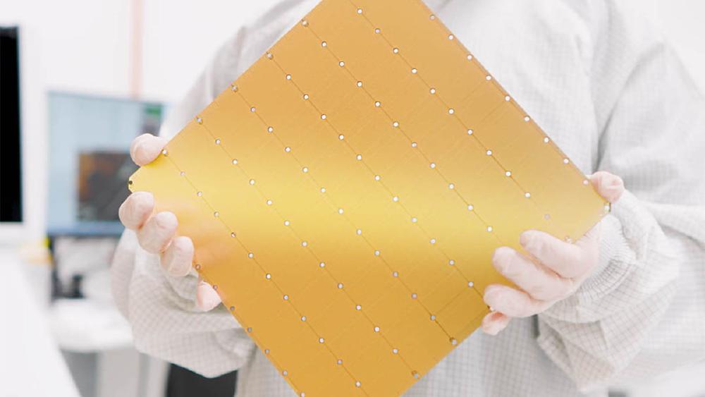
TL;DR
- The largest chip ever manufactured - a single TSMC 5nm wafer with 4 trillion transistors and 900,000 AI-optimized cores
- 44GB of on-chip SRAM with 21 PB/s aggregate bandwidth - no HBM, no off-chip memory bottleneck for on-wafer data
- Around 125 PFLOPS FP8 performance per CS-3 system - roughly 2x the WSE-2
- Signed a $20B agreement with OpenAI for 750 MW of inference capacity; AWS deployed CS-3 systems inside Amazon Bedrock
- Cerebras filed for a Nasdaq IPO in April 2026 at a $22-25B target valuation, on $510M in 2025 revenue
2026 Developments
The past several months changed the commercial picture for Cerebras significantly.
OpenAI. Cerebras announced a $20 billion Master Relationship Agreement with OpenAI covering 750 megawatts of inference compute capacity. This is the largest single customer commitment in the company's history, and it's for the WSE-3 specifically. The agreement validates the chip's inference speed advantage for the workload that matters most commercially right now: serving large language models at scale.
Amazon Bedrock. On March 13, 2026, AWS deployed Cerebras CS-3 systems inside its data centers through Amazon Bedrock. The architecture is disaggregated: AWS Trainium chips handle the prefill phase of inference while Cerebras WSE chips handle the decode phase. The result, according to AWS, is 5x more high-speed token capacity in the same hardware footprint. For Amazon, the Trainium-plus-WSE pairing is a way to use WSE-3's bandwidth advantage where it's most pronounced - in the decode phase, where generation speed is bandwidth-bound - without putting WSE-3 on the harder compute-bound prefill work.
IPO. Cerebras filed its S-1 with the SEC on April 17, 2026, targeting a Nasdaq listing under ticker CBRS at a $22-25B valuation. The S-1 disclosed $510M in 2025 revenue and $237.8M net income - a swing from a $481.6M net loss in 2024. Revenue grew from $24.6M in 2022 to $510M in 2025, largely on the back of the OpenAI deal and Condor Galaxy deployments.
Q1 2024 - Cerebras CS-3 system (WSE-3) released commercially
2024 - Condor Galaxy 1 and 2 launched with G42, 8 combined ExaFLOPS
March 2026 - AWS launches CS-3 inside Amazon Bedrock (prefill/decode disaggregated architecture)
April 2026 - Cerebras files S-1 for Nasdaq IPO, $22-25B target valuation, $510M 2025 revenue
Overview
The Cerebras Wafer-Scale Engine 3 is the most extreme piece of silicon in the AI hardware landscape. While every other accelerator in production - from NVIDIA's H100 to Groq's LPU to Intel's Gaudi 3 - starts with a standard die cut from a wafer, Cerebras skips the cutting step entirely. The WSE-3 is the wafer. A single 300mm TSMC 5nm wafer containing 4 trillion transistors, 900,000 AI-optimized compute cores, and 44GB of on-chip SRAM connected by a fabric running at 21 petabytes per second. There is nothing else like it in the semiconductor industry.
The architectural bet is straightforward: memory bandwidth is the bottleneck for AI workloads, and the fastest memory is the memory that lives on the same die as the compute. By making the die as large as physically possible - the entire wafer - Cerebras can pack enough SRAM next to enough compute cores to keep everything fed without ever touching external memory for on-wafer computations.
The WSE-3 delivers roughly 125 PFLOPS of FP8 performance per CS-3 system, which puts it in the same performance class as large GPU clusters but with a fundamentally different memory hierarchy. Where a GPU cluster moves data across PCIe lanes, NVLink bridges, and InfiniBand networks, the WSE-3 moves data across on-chip wires measured in millimeters.
The third generation WSE improves on the WSE-2 by moving from TSMC 7nm to 5nm, approximately doubling compute density while maintaining the wafer-scale form factor. The CS-3 system that houses the WSE-3 draws roughly 23kW and is designed to be rack-mounted in standard data center environments. Cerebras also offers inference as a service through Cerebras Inference, and has deployed the Condor Galaxy series of AI supercomputers built from clusters of CS-3 systems for partners including G42.
Key Specifications
| Specification | Details |
|---|---|
| Manufacturer | Cerebras |
| Product Family | Wafer-Scale Engine (3rd generation) |
| Chip Type | Wafer-Scale Processor |
| Process Node | TSMC 5nm |
| Die Size | Full 300mm wafer (~46,225 mm2) |
| Transistors | 4 trillion |
| AI Cores | 900,000 |
| On-Chip Memory | 44GB SRAM |
| On-Chip Bandwidth | 21 PB/s |
| External Memory | None on-wafer (MemoryX off-wafer for model weights) |
| FP16 Performance | ~62 PFLOPS (per CS-3 system, estimated) |
| FP8 Performance | ~125 PFLOPS (per CS-3 system) |
| System TDP | ~23kW (CS-3 system) |
| Intra-Wafer Interconnect | On-wafer 2D mesh fabric |
| Inter-System Interconnect | SwarmX |
| External Storage | MemoryX (for model weights exceeding 44GB) |
| Target Workload | Training and Inference |
| System Price | ~$2-3M (CS-3) |
| Release | Q1 2024 |
Performance Benchmarks
| Metric | Cerebras CS-3 (WSE-3) | NVIDIA DGX H100 (8x H100) | NVIDIA DGX B200 (8x B200) | AMD MI300X (8-GPU) |
|---|---|---|---|---|
| FP8 PFLOPS (system) | ~125 | 31.6 | 72 | 20.9 |
| On-chip/HBM Memory | 44GB SRAM | 640GB HBM3 | 1,440GB HBM3e | 1,536GB HBM3 |
| Memory Bandwidth | 21 PB/s | 26.4 TB/s | 64 TB/s | 41.6 TB/s |
| System Power | ~23kW | ~10.2kW | ~14.3kW | ~10.4kW |
| Approx. System Price | ~$2-3M | ~$300-400K | ~$400-500K (est.) | ~$250-350K |
| LLM Training (relative) | High (sparse/dense) | Baseline | ~2x baseline | ~0.8x baseline |
| Inference Latency (single stream) | Very low | Low | Low | Low |
| PFLOPS per Watt | ~5.4 | ~3.1 | ~5.0 | ~2.0 |
The comparison requires nuance. On raw FP8 FLOPS, the CS-3 has a 4x advantage over a DGX H100 and roughly 1.7x over a DGX B200. But the CS-3 costs 5-8x more than a DGX H100, and the 44GB of SRAM is a fraction of the 640GB-1,536GB HBM available on GPU systems. This means the WSE-3 excels at compute-bound workloads where data can be efficiently streamed from MemoryX, but the memory capacity limitation requires careful system design for very large models.
Bandwidth - The Real Story
The bandwidth numbers are where the WSE-3 is truly in a different league. 21 PB/s of on-chip bandwidth versus 26-64 TB/s of HBM bandwidth on GPU systems represents a 300-800x advantage.
This isn't a perfectly apples-to-apples comparison - SRAM bandwidth and HBM bandwidth serve different roles in the memory hierarchy - but the practical impact is significant.
In LLM inference, the dominant cost is reading model weights from memory once per token produced. This is the "memory bandwidth bound" regime that limits GPU inference speed. On a H100, reading 70GB of model weights at 3,350 GB/s takes about 21ms per token - setting a hard floor on generation speed regardless of how many FLOPS the GPU has.
The WSE-3's 21 PB/s on-chip bandwidth reduces this floor dramatically for weights that reside in SRAM. For a model that fits completely in the 44GB on-chip memory (roughly a 20B parameter model at FP16, or a 40B model at FP8), the bandwidth advantage translates directly into faster token generation.
For models that exceed 44GB - which includes basically all production LLMs at FP16 precision - the MemoryX external storage system becomes the bandwidth bottleneck. Cerebras hasn't published MemoryX bandwidth specifications, which means the actual inference speed for large models depends on a bandwidth figure the company hasn't disclosed. This is a meaningful gap in the publicly available data.
Training Performance
For training workloads, the WSE-3's advantage is most striking on models that exhibit high compute-to-memory ratios. Dense matrix multiplications, convolutions, and attention computations that can be decomposed across the 900,000 cores benefit from the massive parallelism and on-chip bandwidth.
Cerebras has published training benchmarks showing competitive or superior performance to GPU clusters for models including GPT-3 (175B parameters), Llama 2 (70B), and various scientific computing workloads. The company reports near-linear scaling efficiency for data-parallel training, which suggests that the on-chip interconnect fabric provides sufficient bandwidth for gradient synchronization across the 900,000 cores.
The sparsity advantage is also significant. The WSE-3's fine-grained parallel architecture can exploit structured and unstructured sparsity more efficiently than GPUs, because each of the 900,000 cores can independently skip zero-valued computations without the warp-synchronization overhead that limits GPU sparsity performance. Cerebras claims 2-4x speedups on sparse workloads compared to dense equivalents.
Key Capabilities
Wafer-Scale Integration. The defining feature of the WSE-3 is that it's manufactured as a single piece of silicon. Standard chips are cut from a wafer, packaged individually, and then connected on circuit boards through PCIe slots, socket mounts, or interposers. The WSE-3 skips all of that - the entire wafer is the chip.
This removes the packaging overhead, inter-chip communication latency, and bandwidth constraints that limit traditional multi-chip systems. Data moving between two cores on the WSE-3 travels across on-wafer wires, not through PCIe traces, bridge chips, or network cables. The latency and bandwidth of on-wafer communication is orders of magnitude better than any multi-chip interconnect.
The engineering challenge is immense. A standard 300mm wafer contains billions of transistors, and even at 99.99% yield rates, a wafer with 4 trillion transistors would have millions of defective transistors. Cerebras builds redundancy into the design with spare cores that can be activated to replace any defective units - similar in concept to how SSDs over-provision flash cells to replace worn-out blocks.
The manufacturing process also requires custom wafer-scale packaging, power delivery, and cooling solutions that don't exist in conventional semiconductor production. A single wafer-scale chip needs uniform power delivery across a 300mm diameter surface and uniform cooling to prevent thermal hotspots from throttling performance.
The fact that Cerebras ships production CS-3 systems proves that wafer-scale integration is viable as a commercial technology. No other company has attempted this approach at production scale, which means Cerebras has a multi-year head start on the manufacturing learning curve.
MemoryX and SwarmX. The 44GB of on-chip SRAM isn't enough to hold the parameters of large language models at full precision. A 70B parameter model in FP16 requires 140GB - more than 3x the on-chip capacity. A 405B model requires 810GB. Cerebras addresses this with MemoryX, an external memory subsystem that stores model weights and streams them to the WSE-3 during computation.
MemoryX uses high-bandwidth memory modules located outside the WSE-3 wafer but connected via a dedicated high-bandwidth link. The weights are streamed to the WSE-3 on demand, layer by layer, as the computation. The 44GB of on-chip SRAM is a working buffer for the current layer's activations and intermediate results, while MemoryX provides the backing store for the full model.
SwarmX is the interconnect fabric that enables multiple CS-3 systems to work together on a single training job. It handles gradient synchronization for data-parallel training and activation passing for pipeline-parallel training across CS-3 nodes.
Together, MemoryX and SwarmX allow the WSE-3 to train models with trillions of parameters despite the limited on-chip memory. The weights live in MemoryX, the activations and intermediate computations happen on the 44GB SRAM, and the 21 PB/s on-chip bandwidth ensures compute cores are never starved for data during the computation phase.
The MemoryX architecture makes the WSE-3 function as a massive compute engine with a streaming memory interface, rather than a self-contained processor. Model weights flow into the chip, computations happen completely on-chip at 21 PB/s, and results flow back out. This is a fundamentally different execution model than GPUs, where weights, activations, and intermediate results all compete for the same HBM bandwidth.
Cerebras Inference. Cerebras offers inference as a service through their cloud platform, where the WSE-3's massive on-chip bandwidth translates to very fast token generation for LLM serving.
For models that fit in the 44GB SRAM (approximately a 20B parameter model at FP16, or a 40B model at FP8), inference runs completely on-chip with no external memory bottleneck. Cerebras has demonstrated inference speeds passing 1,000 tokens per second on Llama-class models, competitive with Groq's LPU on single-stream latency.
For larger models that require MemoryX streaming, inference performance depends on the MemoryX-to-WSE bandwidth, which Cerebras hasn't published. This is the key unknown for evaluating Cerebras Inference on production-scale models.
The inference service is available through the Cerebras API with per-token pricing, providing cloud access to WSE-3 performance without requiring a $2-3M hardware purchase.
Condor Galaxy Supercomputers. Cerebras has deployed large-scale supercomputer installations built from clusters of CS-3 systems. The Condor Galaxy series, built in partnership with G42 (an Abu Dhabi-based technology company), combines hundreds of CS-3 nodes into multi-exaflop AI supercomputers.
Condor Galaxy 1 and 2 together provide 8 EXAFLOPS of combined AI compute - enough to train Frontier-scale models from scratch. These installations demonstrate that the WSE-3 scales beyond individual systems into cluster-scale infrastructure.
For organizations that need supercomputer-class training capability but want an alternative to NVIDIA-dominated GPU clusters, the Condor Galaxy model provides a turnkey solution. G42, Mayo Clinic, and other Cerebras partners have used these clusters for large-scale model training and scientific computing workloads.
Architecture Deep Dive
The Scale of the WSE-3
To appreciate the WSE-3, consider the numbers in context:
| Metric | WSE-3 | NVIDIA H100 | Ratio |
|---|---|---|---|
| Die area | ~46,225 mm2 | 814 mm2 | 57x |
| Transistors | 4 trillion | 80 billion | 50x |
| Compute cores | 900,000 | 132 SMs | ~6,800x |
| On-chip SRAM | 44GB | ~50MB (L2) | ~880x |
| On-chip bandwidth | 21 PB/s | ~12 TB/s (L2) | ~1,750x |
The H100 is considered a large chip by industry standards. The WSE-3 is 57x larger. The number of independent compute cores - 900,000 - is more than the total number of CUDA cores across an entire 8-GPU DGX H100 node (8 x 16,896 = 135,168 CUDA cores).
The 2D Mesh Fabric
The 900,000 cores on the WSE-3 are connected by a 2D mesh interconnect fabric that spans the entire wafer. Each core can communicate directly with its neighbors in all four cardinal directions (north, south, east, west), and the mesh routing protocol handles multi-hop communication for cores that are not directly adjacent.
The mesh topology is well-suited for the communication patterns of neural network training:
- Data-parallel gradient reduction: Reduce operations can be mapped to efficient tree-based Communication patterns on the 2D mesh
- Tensor parallelism: Adjacent cores can share activation data with minimal latency
- Pipeline parallelism: Layers assigned to contiguous regions of the mesh can stream activations Through the pipeline with near-zero communication overhead
The 21 PB/s aggregate bandwidth represents the total capacity of all mesh links on the wafer operating simultaneously. Individual core-to-core bandwidth is lower, but the aggregate throughput matters because neural network training involves distributed computation across all 900,000 cores simultaneously.
Yield and Redundancy
Semiconductor manufacturing is inherently imperfect. At TSMC's 5nm node, even with excellent process control, a wafer will have defective transistors. For a standard chip with a few hundred mm2 of die area, the probability of a defect is low enough that the majority of dies on a wafer are functional.
For the WSE-3, which uses the entire wafer, every defect that would have killed a standard die is present on the chip. Cerebras handles this through redundancy - the wafer includes more cores and more SRAM than the nominal specifications. Defective cores are identified during testing and replaced with spare cores from the redundancy pool. The mesh interconnect is also designed to route around defective links.
This redundancy approach has a cost: some fraction of the wafer's area is "wasted" on spare cores that aren't used on defect-free wafers. But it enables the fundamental breakthrough of wafer-scale computing by making yield management tractable.
Pricing and Availability
The CS-3 system is priced at approximately $2-3 million per unit, making it a capital expenditure that only large enterprises, research institutions, and well-funded AI labs can justify.
| System | Approx. Price | FP8 Performance | Price per PFLOPS |
|---|---|---|---|
| Cerebras CS-3 (WSE-3) | ~$2.5M | ~125 PFLOPS | ~$20K/PFLOPS |
| NVIDIA DGX H100 (8x H100) | ~$350K | 31.6 PFLOPS | ~$11K/PFLOPS |
| NVIDIA DGX B200 (8x B200) | ~$450K | 72 PFLOPS | ~$6.3K/PFLOPS |
On a pure price-per-PFLOPS basis, the CS-3 is more expensive than GPU alternatives. The NVIDIA DGX B200 is roughly 3x more cost-efficient per FLOP. The value proposition for the CS-3 lies elsewhere.
The 21 PB/s on-chip bandwidth advantage means that for bandwidth-bound workloads - which includes most LLM inference and many training scenarios - the effective performance per dollar can be notably better than what the raw FLOPS comparison suggests. A GPU cluster with 4x fewer FLOPS but 800x less bandwidth may actually be slower on bandwidth-bound workloads than the CS-3.
For organizations evaluating the CS-3, the decision framework is:
- If your workloads are compute-bound (large-batch training with high arithmetic intensity), GPUs offer better price-performance
- If your workloads are bandwidth-bound (inference, small-batch training, sparse models), the WSE-3's architectural advantage closes the price-performance gap or tips it in Cerebras's favor
Cloud Access
Cerebras offers cloud access through multiple channels:
- Cerebras Inference: Per-token API access for inference workloads
- Condor Galaxy: Managed supercomputer access through partnerships (G42, others)
- On-premises CS-3: Direct hardware purchase for organizations with the budget and data center Infrastructure
For organizations that can't justify a $2-3M hardware purchase, cloud access provides an alternative path to WSE-3 performance without the capital expenditure.
Who Should Consider the WSE-3
Strong fit:
- Organizations training models at 100B+ parameter scale where bandwidth-bound performance matters
- Research institutions working on sparse model architectures that benefit from fine-grained parallelism
- AI labs that need an alternative to NVIDIA for supply chain diversification
- Scientific computing workloads (drug discovery, climate modeling, molecular dynamics) that map well To the 900,000-core architecture
- Organizations with the budget and data center infrastructure for $2-3M systems at 23kW power draw
Weak fit:
- Startups or small teams that can't justify multi-million dollar hardware purchases
- Inference-only deployments where Groq's LPU offers better latency at lower cost
- Teams that depend on the CUDA ecosystem and cannot invest in porting to Cerebras's SDK
- Organizations that need broad cloud availability or multi-provider deployment flexibility
- Workloads where the model fits comfortably in GPU HBM and bandwidth isn't the bottleneck
Strengths
- 21 PB/s on-chip bandwidth is 300-800x higher than any HBM-based solution
- 900,000 cores on a single wafer removes inter-chip communication overhead
- ~125 PFLOPS FP8 per system is 4x a DGX H100 in a single unit
- Wafer-scale redundancy engineering proves full-wafer integration is a viable production technology
- MemoryX and SwarmX allow scaling to trillion-parameter models despite limited on-chip SRAM
- Supports both training and inference - not limited to one or the other
- Cerebras Inference service provides cloud access without the $2-3M hardware purchase
- ~5.4 PFLOPS per watt is among the best energy efficiency ratios in the market
Weaknesses
- $2-3M per CS-3 system limits the buyer pool to well-funded organizations
- 44GB on-chip SRAM is a fraction of the 640GB-1,536GB HBM available on GPU systems
- Price-per-PFLOPS is roughly 2-3x worse than current-generation NVIDIA GPU systems
- MemoryX external storage adds latency and complexity for models exceeding 44GB
- Software ecosystem is far less mature than CUDA - smaller developer community and fewer examples
- Single-vendor dependency with no second-source option for the wafer-scale form factor
- 23kW system power requires significant data center cooling and power infrastructure
Related Coverage
- Groq LPU - Another SRAM-based architecture, optimized purely for inference with deterministic latency
- Intel Gaudi 3 - A more conventional ASIC approach to challenging NVIDIA's GPU dominance
- AWS Trainium2 - The Trainium half of Amazon's Trainium-plus-WSE Bedrock architecture
- AWS Trainium3 - Amazon's next-generation training chip
Sources
✓ Last verified May 1, 2026

