AMD Instinct MI455X
AMD's flagship CDNA 4 AI GPU with 432 GB HBM4, 40 PFLOPS FP4, and 2nm chiplet design targeting H2 2026.
The AMD Instinct MI455X is the flagship of the MI400 series and AMD's most ambitious data center GPU to date. Built on CDNA 4 architecture, it uses a heterogeneous chiplet design with compute dies on TSMC 2nm and I/O dies on TSMC 3nm, packing 320 billion transistors across the package. The MI455X is designed specifically for AMD's Helios rack system - a purpose-built 72-GPU architecture that competes directly with NVIDIA's GB300 NVL72. At 40 PFLOPS FP4 per chip and 432 GB of HBM4 memory at 19.6 TB/s, the MI455X represents a generational jump in raw specs. Whether AMD can translate those specs into real-world workload performance - and whether ROCm can keep up - is the more interesting question heading into H2 2026.
TL;DR
- 432 GB HBM4 across 12 stacks at 19.6 TB/s - enough on-chip memory to hold a 405B FP8 model's weights and substantial KV cache on a single GPU
- 40 PFLOPS FP4 and 20 PFLOPS FP8 per chip - AMD claims 10x performance over the MI355X, which is a bold number that deserves skepticism until independent benchmarks arrive
- TSMC 2nm compute chiplets (2 GCDs) + TSMC 3nm I/O dies (2 MCDs) + 16 HBM4 stacks in a single package
- Helios rack: 72 MI455X GPUs = 2.9 FP4 exaFLOPS, 31 TB HBM4, 1.4 PB/s aggregate bandwidth per rack
- 3.6 TB/s scale-up bandwidth via Infinity Fabric + UALink; 300 GB/s scale-out via Ultra Ethernet
- Targeted for H2 2026; pricing not announced
Overview
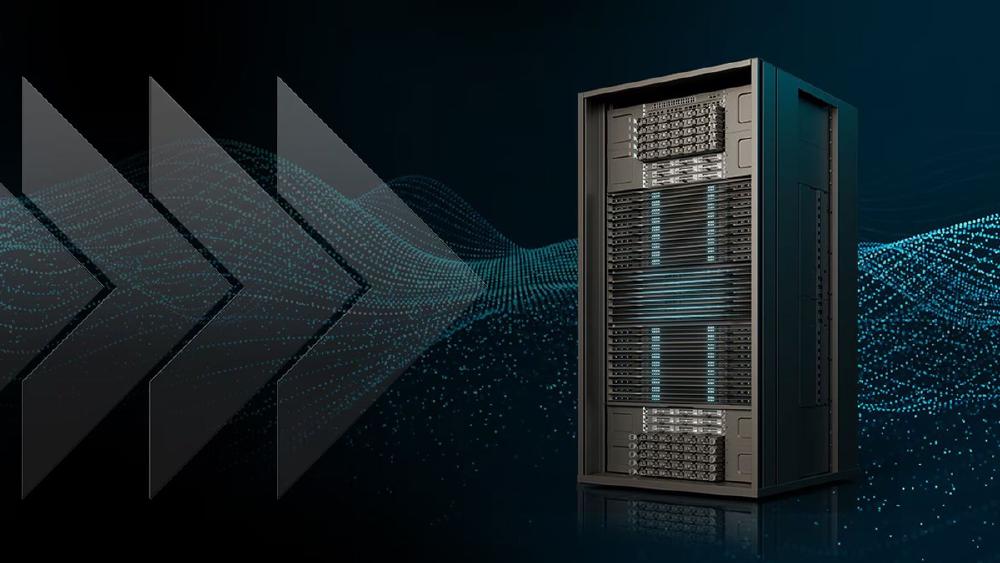
The MI455X sits at the top of the MI400 family alongside the MI440X (enterprise OAM form factor) and the MI430X (HPC/FP64 variant). All three share CDNA 4 silicon and HBM4 memory. The distinction for the MI455X is its deployment target: it's designed to live inside AMD's Helios rack, a 72-GPU system that requires purpose-built infrastructure, much like NVIDIA's NVL72 racks. This isn't a card you drop into an existing server - it's a rack-scale commitment.
The chiplet design is the most technically interesting aspect of the MI455X. AMD uses 2 Graphics Compute Dies (GCDs) on TSMC N2 and 2 Memory Controller Dies (MCDs) on TSMC N3P, bonded together with 16 HBM4 stacks. The decision to mix process nodes - compute on leading-edge 2nm, I/O on mature 3nm - is a cost and yield optimization. TSMC N2 delivers the transistor density needed to maximize compute throughput per watt; N3P is proven, cheaper, and sufficient for the memory controller and Infinity Fabric logic that doesn't need 2nm density. AMD ran a similar playbook with the MI300X, and it paid off in production yield and pricing relative to a hypothetical monolithic approach.
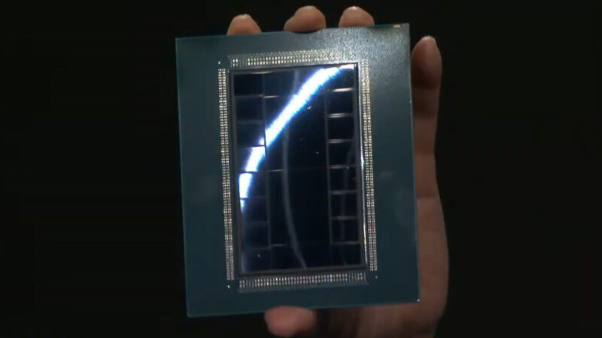 The AMD Instinct MI455X chip package, shown at CES 2026. The package integrates 2 GCDs (TSMC 2nm) and 2 MCDs (TSMC 3nm) with 16 HBM4 stacks.
Source: servethehome.com
The AMD Instinct MI455X chip package, shown at CES 2026. The package integrates 2 GCDs (TSMC 2nm) and 2 MCDs (TSMC 3nm) with 16 HBM4 stacks.
Source: servethehome.com
The memory subsystem is AMD's clearest competitive advantage. 432 GB at 19.6 TB/s puts the MI455X clearly ahead of the NVIDIA GB300 NVL72 on a per-GPU memory capacity basis (288 GB HBM3e per B300 GPU). For inference workloads where model size determines how many GPUs you need, capacity wins directly translate to cost savings: a 405B FP8 model that needs 2 GB300 GPUs fits on 1 MI455X. The bandwidth story is closer - 19.6 TB/s per MI455X versus 22 TB/s per B300 GPU - where NVIDIA maintains an edge.
AMD's claimed 10x improvement over the MI355X is the spec that demands scrutiny. The MI355X was already competitive with GB200-class hardware in LLM inference benchmarks at FP4 precision. A genuine 10x improvement would put the MI455X at roughly 10x GB200 performance levels - an extraordinary claim that AMD hasn't yet backed with third-party benchmarks. The 10x figure likely reflects theoretical FP4 peak compute and favorable memory bandwidth scaling rather than a 10x improvement in end-to-end workload throughput. Real-world gains on training jobs and inference serving will depend heavily on ROCm software maturity, compiler optimization, and whether AMD's new architecture maps cleanly to the dominant model architectures.
Key Specifications
| Specification | Details |
|---|---|
| Manufacturer | AMD |
| Product Family | Instinct MI400 / CDNA 4 |
| Architecture | CDNA 4 |
| Process Node | TSMC 2nm (N2) compute chiplets + TSMC 3nm (N3P) I/O dies |
| Transistors | 320 billion |
| Chiplet Configuration | 2 GCDs (compute) + 2 MCDs (memory controller) + 16 HBM4 stacks |
| GPU Memory | 432 GB HBM4 (12 x 36 GB stacks) |
| Memory Bandwidth | 19.6 TB/s (19,600 GB/s) |
| FP4 Performance | 40 PFLOPS per chip |
| FP8 Performance | 20 PFLOPS per chip |
| FP16 / BF16 Performance | Not publicly disclosed |
| Scale-up Bandwidth | 3.6 TB/s (Infinity Fabric + UALink) |
| Scale-out Bandwidth | 300 GB/s per GPU (Ultra Ethernet) |
| Interconnect | Infinity Fabric + UALink |
| TDP | Not disclosed |
| System | AMD Helios (72-GPU rack) |
| Target Workload | Training and Inference |
| Release Date | H2 2026 |
| Pricing | Not announced |
Helios Rack-Level Specifications
| Metric | Value |
|---|---|
| GPUs per Rack | 72 x MI455X |
| FP4 Compute | 2.9 exaFLOPS |
| FP8 Compute | 1.4 exaFLOPS |
| Total HBM4 Memory | 31 TB |
| Aggregate Bandwidth | 1.4 PB/s |
Performance Benchmarks
Direct MI455X benchmark data isn't available yet - AMD hasn't released the hardware, and no third-party testing exists as of March 2026. The numbers below are context for what AMD has claimed and what reasonable projections look like based on predecessor data.
| Metric | MI355X | MI455X (AMD claimed) | NVIDIA B300 per GPU |
|---|---|---|---|
| FP4 Peak (TFLOPS) | ~7,200 | 40,000 | ~50,000 (sparse) |
| FP8 Peak (TFLOPS) | ~3,600 | 20,000 | ~17,500 |
| Memory Capacity | 288 GB HBM3e | 432 GB HBM4 | 288 GB HBM3e |
| Memory Bandwidth | ~6,000 GB/s | 19,600 GB/s | 22,000 GB/s |
| Process Node | TSMC 3nm | TSMC 2nm/3nm | TSMC 4NP |
Important caveat: AMD's 10x claim over the MI355X is unverified. The MI355X ran Llama 3.1 405B at FP4 at competitive throughput rates against the GB200 - AMD confirmed this in internal testing, and external inference benchmarks showed broadly comparable performance. If the MI455X truly delivers 10x on that workload, it would be the fastest single-chip AI accelerator by a large margin. That's possible given HBM4's 3.3x bandwidth improvement and the architectural advances in CDNA 4, but real-world training and inference efficiency depend on factors that don't scale linearly with peak compute.
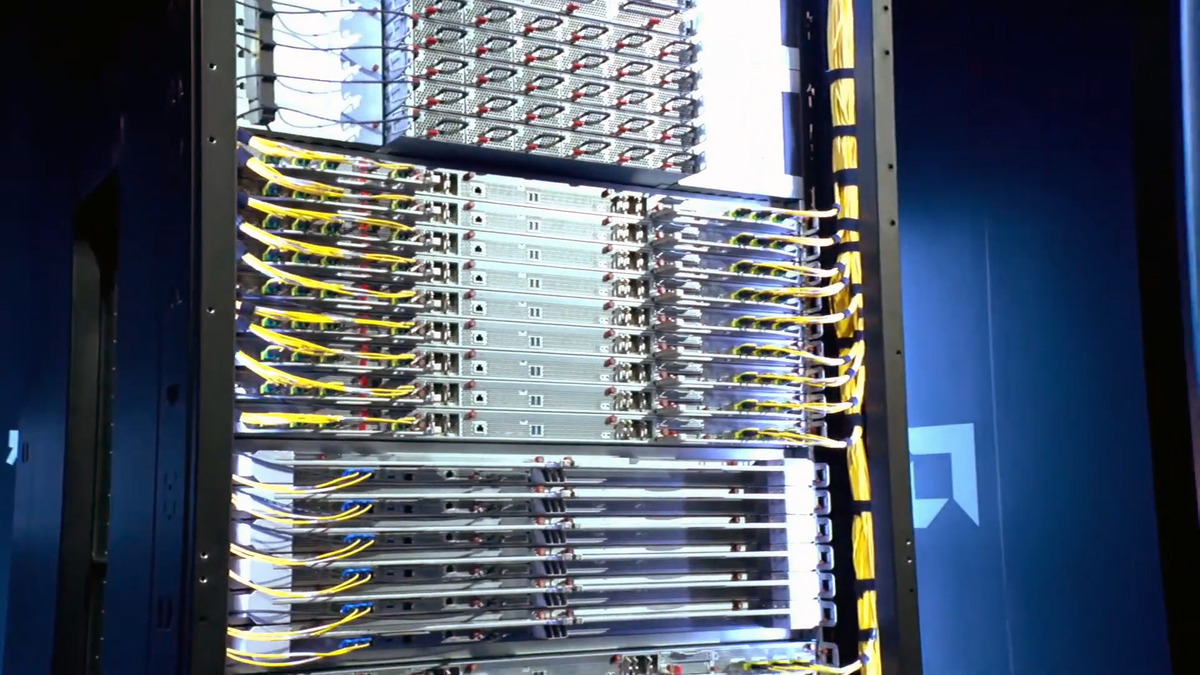 The AMD Helios rack holds 72 MI455X accelerators and delivers 2.9 FP4 exaFLOPS at the rack level.
Source: servethehome.com
The AMD Helios rack holds 72 MI455X accelerators and delivers 2.9 FP4 exaFLOPS at the rack level.
Source: servethehome.com
For comparison context: the GB300 NVL72 rack delivers roughly 1.5 exaFLOPS FP4 across 72 B300 GPUs. A single Helios rack at 2.9 exaFLOPS FP4 would represent nearly a 2x rack-level compute advantage - if AMD's per-chip FP4 numbers hold up. NVIDIA's sparse FP4 compute figures (which use 2:4 sparsity to double throughput) may not be directly comparable to AMD's dense FP4 numbers, which would narrow or eliminate that gap depending on workload sparsity patterns.
Key Capabilities
CDNA 4 on TSMC 2nm. The MI455X is AMD's first data center GPU with compute chiplets on TSMC's N2 process. Compared to the MI355X's 3nm chiplets, N2 delivers better transistor density and per-watt efficiency. The 320 billion transistor count across the package is a significant jump and reflects both the node improvement and the multi-die integration. AMD has chosen to expose this as 2 large GCDs rather than the 8 XCDs used in the MI440X's OAM configuration - a topology decision that affects how the GPU appears to software and how inter-CU communication is handled.
432 GB HBM4 at 19.6 TB/s. HBM4 is a generational leap over HBM3e. The 12 stacks at 36 GB each deliver 3.3x the bandwidth of the MI355X's memory subsystem and a 50% capacity increase. For memory-bound workloads - which includes most LLM inference at large batch sizes - this bandwidth improvement is as important as the compute throughput increase. The 432 GB capacity means single-chip deployment of 400B+ parameter models at FP8 precision, which is a qualitative threshold that changes how clusters are sized for inference.
3.6 TB/s Scale-Up via Infinity Fabric + UALink. The chip-to-chip interconnect within the Helios rack uses AMD's Infinity Fabric with UALink, the open interconnect standard backed by AMD, Intel, Google, Microsoft, and Meta. UALink is a direct challenge to NVIDIA's proprietary NVLink ecosystem. At 3.6 TB/s per chip for scale-up, the Helios rack's 72 GPUs can share data at rates that support large-scale model parallelism. For scale-out (rack-to-rack), 300 GB/s per GPU over Ultra Ethernet is lower than NVLink's per-GPU bandwidth but operates over an open, standard network fabric.
Helios Rack-Scale Architecture. The MI455X is designed to operate as part of a 72-GPU rack, not as a standalone accelerator. This mirrors NVIDIA's NVL72 strategy and represents AMD's acknowledgment that frontier AI training requires thinking at the rack level. Helios delivers 2.9 FP4 exaFLOPS and 31 TB of HBM4 per rack. For large model training, rack-level design choices - power delivery, cooling density, interconnect topology - matter as much as per-chip performance. AMD has shown the hardware at CES 2026 and confirmed the rack design, but detailed thermal and power specs haven't been published.
FP4 and Quantization Support. The MI455X supports FP4 natively, which is the precision level that's becoming standard for production inference of large models. At 40 PFLOPS FP4, the MI455X can serve clearly more inference requests per second than FP8 configurations if model quality at FP4 is acceptable. For models where that's acceptable - which is increasingly the case for 70B+ parameter models after calibration - FP4 inference on the MI455X represents the maximum throughput the hardware can deliver.
Pricing and Availability
AMD hasn't announced pricing for the MI455X. The MI355X was estimated at $15,000 to $20,000 per card; the MI455X, with its HBM4 memory (carrying a first-generation cost premium), TSMC 2nm compute dies, and Helios-specific form factor, will almost certainly be more expensive. Industry analysts expect MI400 series pricing to range from $25,000 to $45,000 per accelerator, with the MI455X at the higher end given its flagship positioning.
| Detail | Information |
|---|---|
| Per-GPU Price | Not announced |
| Expected Range | $25,000-$45,000 (analyst estimates) |
| System | AMD Helios rack (72-GPU) |
| Helios Rack Price | Not announced |
| Target Availability | H2 2026 |
| Cloud Availability | Not confirmed |
Availability is targeted for H2 2026. AMD publicly confirmed the MI400 series and Helios rack remain on schedule at a February 2026 analyst event. Cloud provider availability is less certain - hyperscalers that have launched MI300X (Microsoft Azure, Oracle Cloud) are plausible early adopters, but whether those deployments will use MI455X in Helios racks or MI440X in standard OAM configurations hasn't been disclosed. AMD's data center GPU track record on delivery timelines has been mixed: the MI300X shipped on schedule, but AMD has had prior slips on enterprise GPU programs.
Strengths and Weaknesses
Strengths
- 432 GB HBM4 at 19.6 TB/s - highest memory capacity of any single AI accelerator announced for 2026, enabling single-chip 400B+ parameter model deployment at FP8
- 40 PFLOPS FP4 per chip - if confirmed, competitive with or better than the B300 GPU's dense FP4 throughput
- TSMC 2nm compute chiplets - a full node advantage over the GB300's 4NP process on compute dies
- 2-GCD chiplet design reduces yield risk compared to a monolithic die of equivalent size
- UALink support provides an open-standard alternative to NVLink for scale-out interconnect
- 3.6 TB/s scale-up bandwidth supports large tensor-parallel configurations within the Helios rack
- FP4, FP8, BF16, FP16 precision support covers the full quantization range used in production
Weaknesses
- No TDP disclosed - AMD hasn't published power consumption or cooling requirements, making infrastructure planning difficult
- No pricing announced - cost-per-TFLOP and TCO comparisons are impossible until AMD publishes numbers
- 10x MI355X improvement claim is unverified and likely reflects peak compute scaling rather than workload throughput
- ROCm software ecosystem trails CUDA in optimization depth, inference engine support, and developer tooling
- Helios-specific form factor requires purpose-built rack infrastructure - not compatible with existing OAM server deployments
- Scale-out bandwidth at 300 GB/s per GPU (Ultra Ethernet) is lower than NVLink bandwidth for cross-rack connectivity
- Memory bandwidth (19.6 TB/s) trails the B300 GPU's 22 TB/s - a gap that matters for bandwidth-bound inference workloads
- H2 2026 availability is a broad window; actual hardware in customer hands could be Q4 2026 or early 2027
Related Coverage
- AMD Instinct MI440X - The enterprise OAM variant of the MI400 family for standard 8-GPU server deployments
- AMD Instinct MI350X - The CDNA 4 predecessor with 288 GB HBM3e that the MI455X replaces
- NVIDIA GB300 NVL72 - NVIDIA's rack-scale competitor with 72 B300 GPUs and NVLink interconnect
Sources
- ServeTheHome - AMD EPYC Venice and Instinct MI455X at CES 2026
- Tom's Hardware - AMD Touts Instinct MI430X, MI440X, and MI455X AI Accelerators
- AMD Newsroom - AMD and Partners Share Vision for AI at CES 2026
- The Next Platform - AMD Says Helios Racks and MI400 Series GPUs On Track for H2 2026
- Chips and Cheese - CES 2026: Taking the Lids Off AMD's MI400
- Network World - AMD Launches On-Prem AI Chip at CES
✓ Last verified March 15, 2026

