AMD Instinct MI450 - 2nm, 432 GB HBM4, 40 PFLOPS
AMD's CDNA 5 accelerator on TSMC 2nm with 432 GB HBM4 memory - the GPU behind OpenAI's 1GW deployment and Oracle's 50,000-chip supercluster.
The AMD Instinct MI450 is the commercial flagship of AMD's MI400 series - the GPU that carries AMD's most credible challenge yet against NVIDIA's Vera Rubin platform. Built on CDNA 5 architecture with compute chiplets on TSMC's 2nm N2 node and I/O dies on N3P, it packs 432 GB of HBM4 at 20 TB/s into a package that AMD is positioning as the go-to choice for hyperscale AI deployments.
TL;DR
- AMD's first AI GPU on TSMC 2nm - CDNA 5 architecture, 320 billion transistors across 12 compute chiplets
- 432 GB HBM4 at 20 TB/s gives the MI450 a 50% memory capacity edge over NVIDIA Vera Rubin's 288 GB
- NVIDIA still leads on raw compute: 50 PFLOPS FP4 (Vera Rubin) vs 40 PFLOPS FP4 (MI450)
- OpenAI 6GW deal and Oracle 50,000-GPU commitment confirm hyperscaler buy-in ahead of H2 2026 launch
AMD built the MI450 as a ground-up response to what the Blackwell generation revealed: at frontier scale, memory is often the binding constraint, not compute. A 405B-parameter FP8 model requires roughly 405 GB to hold its weights alone. The MI450 fits that on a single GPU with room for major KV cache; the Vera Rubin R200 doesn't. That architectural bet is the central claim AMD is making with this chip.
The product family naming is worth clarifying upfront. AMD previewed the MI400 series at CES 2026 under three variant names: the MI430X (HPC and sovereign AI with full FP64 support), the MI440X (enterprise on-premises deployments), and the MI455X (the OAM-format variant purpose-built for the Helios rack). The MI450 is AMD's primary go-to-market SKU name for cloud and hyperscaler deployments - sharing the same CDNA 5 silicon and specs but packaged and positioned for broader availability outside of Helios-specific rack deployments.
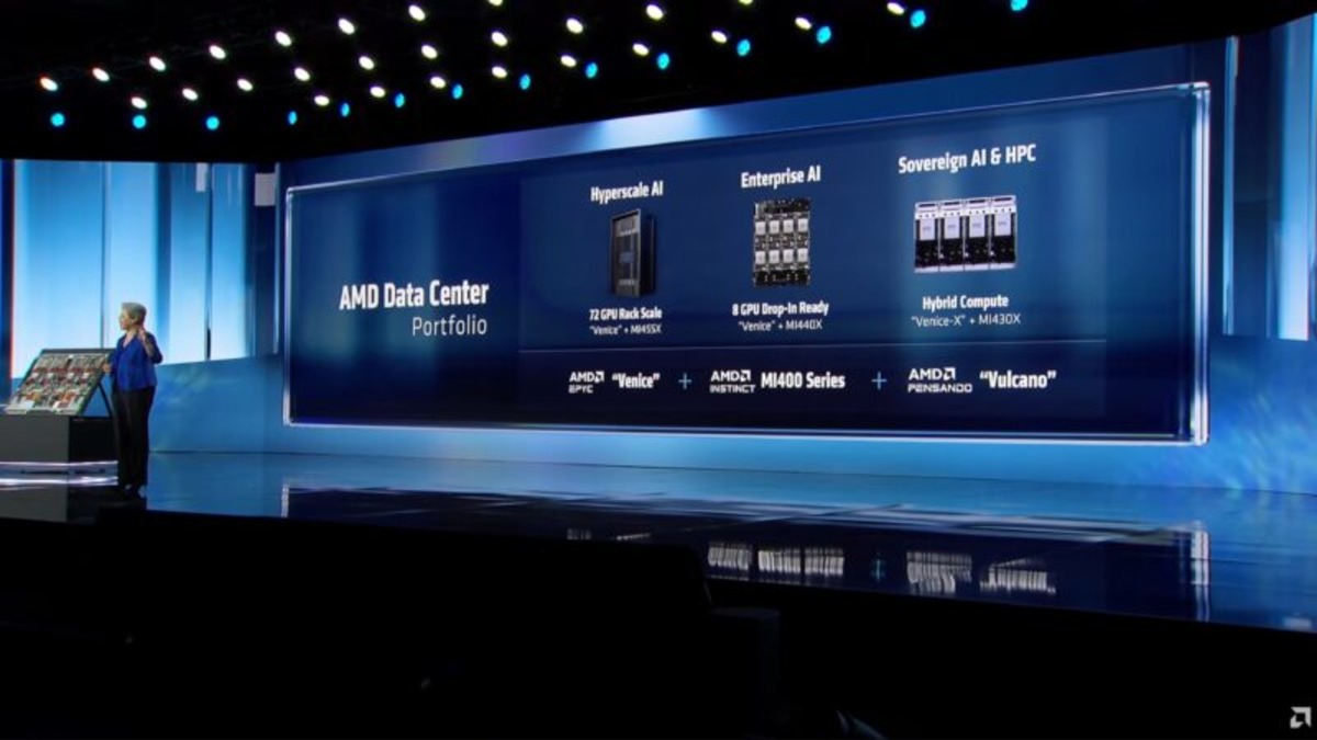 AMD's MI400 series data center portfolio presented at CES 2026, showing the full CDNA 5 accelerator lineup.
Source: servethehome.com
AMD's MI400 series data center portfolio presented at CES 2026, showing the full CDNA 5 accelerator lineup.
Source: servethehome.com
Key Specifications
| Specification | Details |
|---|---|
| Manufacturer | AMD |
| Product Family | Instinct MI400 / CDNA 5 |
| Chip Type | GPU (data center) |
| Architecture | CDNA 5 |
| Process Node | TSMC N2 (compute dies) + TSMC N3P (I/O dies) |
| Transistors | 320 billion (12 compute chiplets + 3 I/O chiplets) |
| Memory | 432 GB HBM4 (12 × 36 GB stacks) |
| Memory Bandwidth | 20 TB/s |
| FP4 Performance | 40,000 TFLOPS (40 PFLOPS) |
| FP8 Performance | 20,000 TFLOPS (20 PFLOPS) |
| Scale-Up Bandwidth | 3.6 TB/s (intra-node) |
| Scale-Out Bandwidth | 300 GB/s (inter-node) |
| TDP | Not disclosed (~1,800W estimated) |
| Target Workloads | AI Training and Inference |
| Release Date | H2 2026 |
Performance Benchmarks
The MI450 hasn't shipped today, so independent benchmark results don't exist yet. What's available are AMD's vendor-stated performance figures and a few clear comparisons against the NVIDIA Vera Rubin R200, which is also shipping in H2 2026.
| Metric | AMD MI450 | NVIDIA Vera Rubin R200 | AMD MI350X |
|---|---|---|---|
| FP4 Performance | 40 PFLOPS | 50 PFLOPS | ~16 PFLOPS |
| FP8 Performance | 20 PFLOPS | 25 PFLOPS | ~8 PFLOPS |
| Memory Capacity | 432 GB HBM4 | 288 GB HBM4 | 288 GB HBM3e |
| Memory Bandwidth | 20 TB/s | 22 TB/s | 8 TB/s |
| Scale-Up BW | 3.6 TB/s | ~5.5 TB/s | ~0.9 TB/s |
| Transistors | 320B | 336B | ~200B (est.) |
| Process Node | 2nm / 3nm | 3nm | 3nm |
The compute gap is real: NVIDIA holds a 25% advantage in raw TFLOPS at FP4 and FP8. The memory gap runs in AMD's direction: the MI450 offers 50% more capacity and the edge narrows on bandwidth (22 vs 20 TB/s). For inference on very large models - anything above 300B parameters at FP8 precision - the MI450's 432 GB may be the deciding factor, since spilling weights to host memory kills throughput regardless of peak TFLOPS.
At rack scale, AMD's advantage compounds. A 72-GPU Helios rack holds 31 TB of HBM4 at 1,400 TB/s aggregate bandwidth. A NVIDIA Vera Rubin NVL72 holds 21 TB at 936 TB/s. The Helios rack is physically larger (double-wide) and presumably power-hungry, but for memory-bound MoE inference workloads, the capacity edge could matter more than compute density.
AMD also claims the MI450 enables customers to "train and infer models that are 50% larger than previous generations entirely in-memory." That's a direct swipe at Blackwell: fewer multi-node tensor parallelism hops, lower latency, higher effective throughput for the workloads that dominate AI production today.
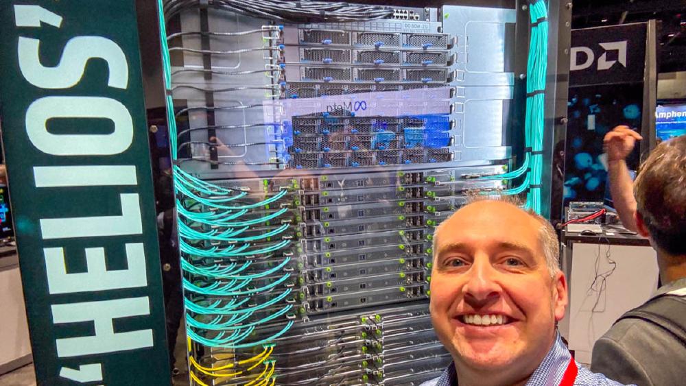
 The AMD Helios rack housing 72 MI450-class GPUs, photographed at OCP Summit 2025.
Source: servethehome.com
The AMD Helios rack housing 72 MI450-class GPUs, photographed at OCP Summit 2025.
Source: servethehome.com
Key Capabilities
The MI450's chiplet architecture is the most technically notable aspect of this generation. The 12 compute chiplets on TSMC N2 are AMD's first AI chips on the 2nm node - beating NVIDIA's Vera Rubin R200, which uses TSMC 3nm across. Chiplet disaggregation lets AMD optimize each die independently: the compute dies get the fastest process node while the I/O dies use the more cost-efficient N3P. Total transistor count reaches 320 billion across the package.
HBM4 at 20 TB/s is a generational step. The MI350X managed 8 TB/s on HBM3e. The MI450 more than doubles that figure, which directly addresses the memory bandwidth wall that becomes critical at inference batch sizes of one to four - the latency-sensitive regime that matters most for production API workloads.
The scale-out interconnect is worth noting separately. At 300 GB/s inter-node bandwidth, the MI450 is designed for large multi-node training clusters where all-reduce communication controls end-to-end training time. This is roughly comparable to NVIDIA's ConnectX-9-based inter-node bandwidth in the Vera Rubin platform. The ROCm software stack, specifically the RCCL collective communication library, is where AMD has historically lost ground - not in hardware specs but in engineering maturity.
Pricing and Availability
AMD hasn't disclosed official pricing. Community estimates put a single MI450 around $27,000-$35,000, which would be broadly following the MI350X's current cloud pricing and competitive with what Vera Rubin is expected to carry. These figures are unconfirmed.
What's confirmed is deployment scale. Oracle Cloud Infrastructure committed to an initial deployment of 50,000 MI450 GPUs starting in Q3 2026, with expansion planned through 2027. That supercluster will be powered by Helios racks combining MI450 GPUs with AMD EPYC Venice CPUs and AMD Pensando Vulcano NICs. OpenAI signed a 6-gigawatt AMD GPU agreement, with the first 1 GW specifically on MI450 hardware beginning in H2 2026.
Both commitments were made before the chips shipped - from AMD's stated specs and qualification silicon. That's meaningfully different from paying for production performance. It's worth watching whether Oracle and OpenAI hit their deployment timelines and whether their workloads map onto AMD's claimed advantages.
Cloud availability for external customers will lag behind these first-party deployments by several months. Expect MI450 instances on major cloud providers in early 2027 at the earliest, based on the pattern from Blackwell and MI350X availability.
Strengths and Weaknesses
Strengths
- Memory capacity lead: 432 GB HBM4 per GPU gives the MI450 a clear edge for large-model inference, especially at low batch sizes where weights dominate memory usage
- First mover on 2nm: TSMC N2 gives AMD a process technology advantage over NVIDIA's Vera Rubin on this generation; next NVIDIA generation (Rubin Ultra) will close that gap
- Hyperscaler validation: OpenAI 6GW and Oracle 50K GPU commitments aren't marketing claims - they represent real procurement decisions and suggest the ROCm software ecosystem has improved enough to pass customer qualification
- Rack-scale memory: The Helios 72-GPU rack's 31 TB aggregate HBM4 exceeds the equivalent NVIDIA NVL72 configuration by 48%, relevant for very large MoE model deployments
Weaknesses
- Lower compute ceiling: 40 PFLOPS FP4 vs 50 PFLOPS for Vera Rubin means compute-bound training workloads (dense transformers, not MoE) favor NVIDIA
- Software ecosystem gap: ROCm's CUDA compatibility layer and library coverage have improved significantly, but CUDA remains the default target for most AI frameworks; porting friction is real
- No independent benchmarks yet: All performance figures come from AMD. Actual LLM inference tokens-per-second data on production workloads won't exist until chips ship in volume
- TDP uncertainty: Power consumption above 1,500W creates real cooling challenges; AMD hasn't disclosed official TDP, which complicates data center planning
Related Coverage
- AMD Instinct MI455X - The OAM-format Helios rack variant of the same CDNA 5 silicon
- AMD Helios Rack - The 72-GPU rack-scale system designed around MI450/MI455X
- AMD Instinct MI430X - HPC and sovereign AI variant with full FP64
- AMD Instinct MI440X - Enterprise on-premises deployment variant
- NVIDIA Vera Rubin NVL144 - AMD's primary competition at rack scale
- AMD and Meta 6GW AI chip deal - Background on AMD's hyperscaler push
- Meta-AMD $100B partnership - Strategic partnership context
Sources:
- AMD CES 2026 Press Release - MI400 Series Announcement
- Oracle to deploy 50,000 AMD Instinct MI450 GPUs - Data Center Dynamics
- AMD Officially Confirms 2nm Process for Instinct MI450 - TechPowerUp
- AMD and Oracle 50,000 MI450 GPU supercluster - Tom's Hardware
- AMD Instinct MI455X at CES 2026 - ServeTheHome
- AMD Helios MI450 Rack at OCP Summit - ServeTheHome
- AMD MI450 vs NVIDIA Vera Rubin - HotHardware
- AMD MI450 2nm process details - TweakTown
- AMD and OpenAI 6GW GPU deal - VideoCardz
- AMD Instinct MI450 claims vs NVIDIA Rubin Ultra - TechRadar
✓ Last verified June 15, 2026
