AMD Instinct MI440X - CDNA 5 Enterprise GPU
Complete specs and analysis of the AMD Instinct MI440X - a CDNA 5 enterprise GPU with 432GB HBM4, 19.6 TB/s bandwidth, and TSMC 2nm compute chiplets.
TL;DR
- 432GB HBM4 memory across 12 stacks at 19.6 TB/s aggregate bandwidth - 1.5x the capacity of the NVIDIA Rubin R200's 288GB
- CDNA 5 architecture on TSMC 2nm (N2) compute chiplets - AMD's first 2nm data center GPU, with 3nm (N3P) I/O dies
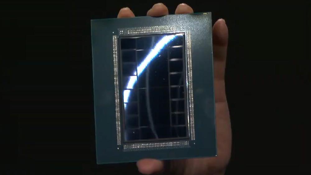
- ~320 billion transistors across a 12-die chiplet package (8 XCDs + active interposer/IO dies) on CoWoS-L
- First AMD GPU with UALink interconnect for open-standard scale-out networking alongside Infinity Fabric
- MI440X is the enterprise 8-GPU variant of the MI400 family - per-chip performance numbers have not been separately disclosed from the MI455X flagship
- Expected H2 2026 availability in OAM form factor, compatible with existing UBB chassis
Overview
The AMD Instinct MI440X is the enterprise-focused member of AMD's MI400 accelerator family, which also includes the MI455X (the flagship, designed for the Helios rack-scale system) and the MI430X (an HPC-oriented variant with strong FP64 capabilities). All three share the same CDNA 5 silicon and HBM4 memory subsystem. The difference is the deployment target: the MI440X ships in the OAM form factor for standard 8-GPU server configurations, while the MI455X is optimized for AMD's proprietary Helios 72-GPU rack architecture.
AMD has not disclosed MI440X-specific compute performance numbers. What we know comes from the MI455X, which AMD confirmed at CES 2026 as delivering 40 PFLOPS FP4, 20 PFLOPS FP8, and 10 PFLOPS FP16 per GPU. AMD describes the MI440X as a "scaled-back MI455X," but hasn't clarified whether "scaled back" means lower clock speeds, disabled compute units, reduced interconnect bandwidth, or simply a different thermal/power profile for the OAM form factor. Until AMD publishes MI440X-specific benchmarks, the MI455X numbers serve as an upper bound.
What's confirmed is the memory subsystem - and it's sizable. The MI440X packs 432GB of HBM4 across 12 stacks at 8 Gbps per pin, delivering 19.6 TB/s of aggregate memory bandwidth. That's 1.5x the capacity and roughly 0.89x the bandwidth of NVIDIA's Rubin R200 (288GB at 22 TB/s). The capacity lead is AMD's competitive wedge here: at FP8 precision, a single MI440X can hold a 405B-parameter model (~405GB) with room for KV cache. The R200 can't fit that model at FP8 on a single chip. This is the same strategic playbook AMD ran with the MI300X and MI350X - win on memory, compete on compute.
Key Specifications
| Specification | Details |
|---|---|
| Manufacturer | AMD |
| Product Family | Instinct MI400 |
| Architecture | CDNA 5 |
| Process Node | TSMC 2nm (N2) compute chiplets + TSMC 3nm (N3P) I/O dies |
| Transistors | ~320 billion (package total; confirmed for MI455X) |
| Chiplet Configuration | 12 dies total - 8 XCDs (compute) + active interposer/IO dies |
| GPU Memory | 432 GB HBM4 (12 stacks x 36GB) |
| HBM4 Per-Pin Rate | 8 Gbps |
| Memory Bandwidth | 19,600 GB/s (19.6 TB/s) |
| FP4 Performance | Up to 40 PFLOPS (MI455X; MI440X TBD) |
| FP8 Performance | Up to 20 PFLOPS (MI455X; MI440X TBD) |
| FP16 / BF16 Performance | Up to 10 PFLOPS (MI455X; MI440X TBD) |
| Supported Precisions | FP4, FP6, FP8, BF16, FP16, FP32 |
| Chip-to-Chip Bandwidth | 3.6 TB/s |
| Scale-Out Bandwidth | 300 GB/s per GPU |
| Interconnect | Infinity Fabric + UALink |
| Packaging | CoWoS-L |
| Form Factor | OAM (fits existing UBB boxes) |
| TDP | Not officially disclosed |
| Target Workload | Training and Inference |
| Release Date | H2 2026 |
| Pricing | Not disclosed |
Note: Performance figures in this table reflect the MI455X flagship. AMD has described the MI440X as a "scaled-back" variant but hasn't published separate per-chip performance numbers. Memory capacity, bandwidth, and architectural features are shared across the MI400 family and are confirmed for the MI440X. This page will be updated when AMD discloses MI440X-specific compute benchmarks.
Performance Benchmarks (Estimated)
| Metric | MI300X | MI350X | MI440X (est.) | NVIDIA B200 | NVIDIA Rubin R200 |
|---|---|---|---|---|---|
| FP8 Peak (TFLOPS) | 2,610 | ~3,600 | Up to 20,000* | 9,000 (dense) | 17,500 |
| FP4 Peak (TFLOPS) | N/A | ~7,200 | Up to 40,000* | 18,000 (sparse) | 50,000 (sparse) |
| Memory Capacity | 192GB | 288GB | 432GB | 192GB | 288GB |
| Memory Bandwidth | 5,300 GB/s | ~6,000 GB/s | 19,600 GB/s | 8,000 GB/s | 22,000 GB/s |
| Process Node | TSMC 5nm/6nm | TSMC 3nm | TSMC 2nm/3nm | TSMC 4NP | TSMC N3P |
| Memory Type | HBM3 | HBM3e | HBM4 | HBM3e | HBM4 |
*MI455X confirmed numbers. MI440X is described as "scaled back" - actual per-chip numbers may be lower.
The memory capacity story is clear. At 432GB, the MI440X offers 2.25x the capacity of the B200 and 1.5x the capacity of the Rubin R200. For inference workloads where model size determines how many GPUs you need, this is a direct cost multiplier. A Llama 405B model at FP8 precision requires ~405GB of weight storage - that fits on a single MI440X but requires two R200s. At FP4, even 800B+ parameter models become single-GPU deployable on the MI440X.
The bandwidth comparison is more nuanced. At 19.6 TB/s, the MI440X trails the R200's 22 TB/s by about 11%. For memory-bandwidth-bound workloads like autoregressive LLM decoding, this gap matters. The MI440X partially compensates with its larger memory pool - more capacity means larger batch sizes and more KV cache headroom, which improves throughput by amortizing per-token bandwidth costs across more concurrent requests.
Key Capabilities
CDNA 5 Architecture on TSMC 2nm. The MI440X is AMD's first data center GPU on TSMC's N2 process node for compute chiplets, paired with N3P I/O dies. The 2nm node delivers meaningful transistor density and power efficiency improvements over the 3nm chiplets in the MI350X. AMD packs about 320 billion transistors across the 12-die package - a significant jump from the MI350X's estimated transistor count and competitive with the Rubin R200's 336 billion. The chiplet approach continues to give AMD a manufacturing flexibility advantage: smaller dies yield better than large monolithic designs, and mixing process nodes lets AMD optimize cost versus performance for each die type.
432GB HBM4 at 19.6 TB/s. The MI440X is one of the first GPUs to ship with HBM4, the next-generation high-bandwidth memory standard. Each of the 12 stacks provides 36GB at 8 Gbps per pin, for an aggregate 432GB and 19.6 TB/s. This is a generational leap from the MI350X's HBM3e (288GB at ~6,000 GB/s) - roughly 1.5x the capacity and 3.3x the bandwidth. HBM4's wider interface and higher per-pin data rates enable this jump without proportionally increasing power consumption. The 432GB capacity is, now, the highest of any single AI accelerator announced for the 2026 generation.
UALink - First AMD GPU with Open Interconnect. The MI440X is AMD's first GPU to support UALink alongside Infinity Fabric. UALink is the open-standard interconnect backed by AMD, Intel, Google, Microsoft, Meta, and others as an alternative to NVIDIA's proprietary NVLink. For the MI440X, this means 300 GB/s per GPU of scale-out bandwidth over an industry-standard interface. The chip-to-chip bandwidth (within a node) remains 3.6 TB/s via Infinity Fabric. UALink matters most for organizations building multi-vendor or open-architecture clusters - it removes the lock-in that NVLink creates in NVIDIA deployments.
12-Die Chiplet Design on CoWoS-L. The MI440X uses TSMC's CoWoS-L (chip-on-wafer-on-substrate with local silicon interconnect) advanced packaging to integrate 8 compute chiplets (XCDs) and 4 I/O/interposer dies into a single package. This is a more complex integration than the MI300X's 12-die CoWoS-S design, with CoWoS-L providing higher inter-chiplet bandwidth and more flexible die placement. The active interposer layer enables all 8 XCDs to communicate with low latency, which is critical for maintaining the illusion of a single unified GPU across what is actually a distributed compute fabric.
OAM Form Factor Compatibility. The MI440X ships in the OAM (OCP Accelerator Module) form factor and is designed to drop into existing Universal Baseboard (UBB) server chassis. This is a deliberate choice for enterprise adoption - organizations with existing 8-GPU MI300X or MI350X server infrastructure can upgrade to MI440X without replacing their server hardware. The MI455X, by contrast, targets AMD's Helios rack architecture, which requires a purpose-built 72-GPU system. The MI440X is the option for customers who want CDNA 5 silicon without committing to a full rack-scale redesign.
Pricing and Availability
AMD hasn't announced pricing for any MI400 series variant. Given the TSMC 2nm compute dies, HBM4 memory (which carries a first-generation cost premium), and the 12-die CoWoS-L packaging, the MI440X will almost certainly be more expensive than the MI350X. Industry analysts expect MI400 series pricing in the $25,000 to $45,000 range per accelerator, though the exact positioning of the MI440X within that range is unclear.
| Detail | Information |
|---|---|
| GPU Price (individual) | Not disclosed |
| Expected Range | $25,000-$45,000 (analyst estimates for MI400 series) |
| Form Factor | OAM |
| Server Configuration | 8-GPU UBB chassis |
| Target Availability | H2 2026 |
| OEM Partners | Expected from major server OEMs (Dell, HPE, Lenovo, Supermicro) |
Availability is targeted for H2 2026. AMD showed MI455X and Helios hardware at CES 2026 and confirmed at a February 2026 analyst event that the MI400 series and Helios racks remain on track for the second half of the year. Whether "H2 2026" means initial shipments in Q3 or volume availability in Q4 remains to be seen - AMD's track record on data center GPU launch timelines has been mixed.
Cloud provider availability for the MI440X specifically is uncertain. Hyperscalers like Microsoft Azure and Oracle Cloud, which have adopted previous Instinct generations, are likely candidates for early MI400 deployment. However, the MI455X in the Helios rack configuration may take priority for cloud deployments given its higher compute density per rack, potentially pushing standalone MI440X cloud instances to a later date.
Strengths and Weaknesses
Strengths
- 432GB HBM4 memory - the highest capacity of any single GPU in the 2026 generation, enabling single-chip deployment of 405B+ parameter models at FP8
- 19.6 TB/s memory bandwidth - a 3.3x generational leap over the MI350X, competitive with NVIDIA Rubin
- TSMC 2nm compute chiplets deliver a full node advantage over competitors still on 3nm-class processes
- UALink support provides open-standard scale-out interconnect - a first for AMD GPUs and a meaningful alternative to NVLink lock-in
- OAM form factor fits existing UBB infrastructure, enabling upgrade-in-place for current MI300X/MI350X server deployments
- 12-die chiplet design on CoWoS-L continues AMD's manufacturing cost and yield advantages
- FP4, FP6, FP8 precision support covers the full range of modern quantization strategies
Weaknesses
- MI440X-specific compute performance numbers haven't been disclosed - all TFLOPS figures are MI455X upper bounds
- "Scaled-back MI455X" positioning is vague - the nature and magnitude of the performance reduction is unknown
- ROCm software ecosystem continues to trail CUDA in maturity, developer tooling, and optimization depth
- No official TDP disclosed - power consumption and cooling requirements remain unclear for infrastructure planning
- No pricing information - cost-per-TFLOP and cost-per-GB comparisons are impossible until AMD publishes numbers
- HBM4 is a first-generation memory technology with potential yield constraints and supply allocation risk
- The MI455X in Helios may receive AMD's primary software optimization focus, with MI440X treated as secondary
- Memory bandwidth (19.6 TB/s) trails the Rubin R200's 22 TB/s by 11%, which matters for bandwidth-bound inference
Related Coverage
- AMD Instinct MI300X - The CDNA 3 predecessor that established AMD's memory-capacity-first strategy
- AMD Instinct MI350X - The CDNA 4 generation with 288GB HBM3e and FP4 support
- NVIDIA B200 - Blackwell Flagship GPU - The current-gen NVIDIA flagship with 192GB HBM3e
- NVIDIA Rubin R200 - Next-Gen AI Superchip - NVIDIA's 2026 flagship with 288GB HBM4 and 22 TB/s bandwidth
Sources
- Tom's Hardware - AMD Touts Instinct MI430X, MI440X, and MI455X AI Accelerators
- AMD Newsroom - AMD and Partners Share Vision for AI at CES 2026
- The Next Platform - AMD Says Helios Racks and MI400 Series GPUs On Track for H2 2026
- Chips and Cheese - CES 2026: Taking the Lids Off AMD's MI400
- ServeTheHome - AMD EPYC Venice and Instinct MI455X at CES 2026
- Network World - AMD Launches On-Prem AI Chip at CES
