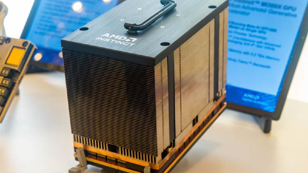
AMD Instinct MI300X
AMD Instinct MI300X specs, benchmarks, and real-world performance data. 192GB HBM3, 5,300 GB/s bandwidth, 2,610 TFLOPS FP8 on CDNA 3 chiplet architecture.
TL;DR
- 192GB HBM3 memory - 2.4x the NVIDIA H100's 80GB - makes it the memory density leader for large model inference
- 5,300 GB/s aggregate memory bandwidth across 8 HBM3 stacks, keeping 2,610 TFLOPS of FP8 compute fed
- TSMC 5nm (XCD compute) + 6nm (IOD) chiplet architecture with 12 chiplets on a single package
- CDNA 3 architecture with 304 compute units and native support for FP8, FP16, BF16, and sparsity
- Street pricing around $10,000-$15,000 - roughly 30-50% less than a comparable NVIDIA H100 SXM
Overview
The AMD Instinct MI300X is the GPU that proved AMD could compete at the data center AI accelerator level. Launched in December 2023, it arrived at exactly the right moment - hyperscalers and enterprises were desperate for alternatives to NVIDIA's supply-constrained H100, and the MI300X delivered a genuine technical argument beyond just "it's available." The 192GB of HBM3 memory on a single accelerator was the headline spec, and it remains the card's strongest selling point for inference workloads where model size exceeds what an 80GB H100 can hold.
The architecture tells a chiplet story. AMD packs 12 dies onto a single package - 8 XCD (Accelerator Complex Die) compute chiplets on TSMC's 5nm node and 4 IOD (I/O Die) chiplets on the 6nm node. Each XCD contains 38 compute units, giving the full package 304 CUs and 19,456 stream processors. The chiplet approach lets AMD scale compute and memory independently, and it's the same design philosophy that revived AMD's CPU business with Ryzen and EPYC. Whether that approach can keep pace with NVIDIA's monolithic reticle-limit designs in future generations is the open question, but for MI300X, it works.
ROCm software maturity is the real conversation. The hardware specs are competitive on paper, but the CUDA ecosystem advantage NVIDIA holds is measured in years of library optimization, framework integration, and developer muscle memory. AMD has made significant progress - PyTorch, JAX, and most major frameworks run on ROCm - but you will still hit edge cases where a CUDA kernel has been hand-tuned and the ROCm equivalent has not. For organizations willing to invest in the software stack, the MI300X offers genuine price-performance advantages. For teams that need everything to work out of the box on day one, the friction is real.
Key Specifications
| Specification | Details |
|---|---|
| Manufacturer | AMD |
| Product Family | Instinct MI300 |
| Architecture | CDNA 3 |
| Process Node | TSMC 5nm (XCD) / 6nm (IOD) |
| Chip Type | GPU |
| Compute Units | 304 |
| Stream Processors | 19,456 |
| FP8 Performance | 2,610 TFLOPS |
| FP16 / BF16 Performance | 1,307 TFLOPS |
| FP32 Performance | 163.4 TFLOPS |
| Memory | 192GB HBM3 |
| Memory Stacks | 8x HBM3 |
| Memory Bandwidth | 5,300 GB/s |
| Infinity Fabric Bandwidth | 896 GB/s (bidirectional) |
| Interconnect | AMD Infinity Fabric |
| TDP | 750W |
| Form Factor | OAM |
| Cooling | Liquid or air (platform dependent) |
| Target Workload | Training and Inference |
| Release Date | December 2023 |
| Estimated Street Price | $10,000-$15,000 |
Performance Benchmarks
| Benchmark / Metric | MI300X | NVIDIA H100 SXM | NVIDIA A100 80GB |
|---|---|---|---|
| FP8 Peak (TFLOPS) | 2,610 | 1,979 | N/A |
| FP16/BF16 Peak (TFLOPS) | 1,307 | 990 | 312 |
| Memory Capacity | 192GB | 80GB | 80GB |
| Memory Bandwidth | 5,300 GB/s | 3,350 GB/s | 2,039 GB/s |
| LLaMA 2 70B Inference (tok/s, single GPU) | ~38-42 | ~22-28 | ~12-15 |
| Llama 70B fits in single GPU memory | Yes | No (requires 2x) | No (requires 2x) |
| Power (TDP) | 750W | 700W | 400W |
| Price (estimated) | $10,000-$15,000 | $25,000-$40,000 | $10,000-$15,000 |
The inference throughput numbers above are approximate and vary significantly by framework, quantization strategy, batch size, and sequence length. The MI300X's advantage is most pronounced on large models (70B+ parameters) where its 192GB memory allows single-GPU deployment of models that require multi-GPU setups on the H100. For smaller models that fit comfortably in 80GB, the H100's more mature software stack and better kernel optimization often close or eliminate the gap.
Training performance is harder to summarize in a single number. On MLPerf Training v3.1, AMD demonstrated competitive results with MI300X clusters, but NVIDIA's DGX H100 systems still hold most of the submission records. The gap narrows at scale when communication overhead becomes a larger factor and AMD's Infinity Fabric interconnect performs well.
Key Capabilities
Memory Density for Large Model Inference. The 192GB HBM3 is the MI300X's killer feature. A Llama 2 70B model in FP16 requires approximately 140GB of memory. On an H100, that means splitting across two GPUs with the associated inter-GPU communication overhead. On the MI300X, it fits on a single accelerator with room to spare for KV cache and batch processing. For inference service providers running 70B-class models, this translates directly to lower infrastructure cost per query. The math is straightforward - one MI300X at $12,000 versus two H100s at $60,000+ for the same model.
Chiplet Architecture Scalability. The 12-chiplet design is not just a manufacturing trick - it's a strategic architecture decision. By separating compute (5nm XCD) from I/O (6nm IOD), AMD can iterate on each independently. The XCD dies are small enough to achieve high yields on TSMC's 5nm process, which keeps costs down. This is the same approach that let AMD price EPYC competitively against Intel Xeon while offering more cores, and it gives AMD a structural cost advantage in silicon. The trade-off is inter-chiplet latency, but AMD's Infinity Fabric has matured enough that this is rarely a bottleneck for AI workloads.
ROCm Ecosystem and Open Software. AMD's ROCm stack is open-source, which matters for organizations that want to avoid vendor lock-in or need to customize their inference pipeline. PyTorch 2.x has first-class ROCm support, vLLM runs on MI300X, and the major cloud providers (Microsoft Azure, Oracle Cloud) offer MI300X instances. The ecosystem is not at CUDA parity - it likely never will be in absolute terms - but it has crossed the threshold of "good enough for production" for most transformer inference workloads.
Pricing and Availability
The MI300X launched at estimated street prices of $10,000 to $15,000, though actual pricing varies significantly by volume and channel. AMD does not publish official MSRPs for data center accelerators. Major OEMs including Dell, HPE, Lenovo, and Supermicro ship MI300X-based systems, and cloud availability includes Microsoft Azure (ND MI300X v5 instances) and Oracle Cloud Infrastructure.
| Accelerator | Estimated Price | Memory | Price per GB |
|---|---|---|---|
| AMD Instinct MI300X | $10,000-$15,000 | 192GB | $52-$78/GB |
| NVIDIA H100 SXM | $25,000-$40,000 | 80GB | $312-$500/GB |
| NVIDIA A100 80GB | $10,000-$15,000 | 80GB | $125-$188/GB |
On a price-per-GB-of-HBM basis, the MI300X is significantly cheaper than the H100. This metric matters most for memory-bound inference workloads. For compute-bound training workloads, price-per-TFLOP is more relevant, and the MI300X is competitive there as well given its lower absolute price.
Availability has been generally better than NVIDIA's H100 throughout 2024, though AMD's total addressable supply is still much smaller. Lead times for MI300X systems have typically been 4-8 weeks versus 6-12+ months for H100 systems during peak demand periods.
Architecture Deep Dive
The MI300X's chiplet architecture deserves a closer look because it is fundamentally different from how NVIDIA builds GPUs - and that difference has real consequences for performance, cost, and future scaling.
Chiplet Topology. The MI300X package contains 12 dies organized in two layers. The bottom layer holds 4 I/O Dies (IODs) fabricated on TSMC's 6nm node. These IODs house the memory controllers, Infinity Fabric links, and PCIe/CXL interfaces. The top layer holds 8 Accelerator Complex Dies (XCDs) on TSMC's 5nm node, stacked on top of the IODs using a silicon interposer. Each XCD contains 38 compute units (CUs) with 64 stream processors each, giving 2,432 stream processors per XCD and 19,456 total across the package.
| Component | Count | Process Node | Function |
|---|---|---|---|
| XCD (Compute Die) | 8 | TSMC 5nm | 38 CUs each, FP8/FP16/BF16/FP32/INT8 compute |
| IOD (I/O Die) | 4 | TSMC 6nm | Memory controllers, Infinity Fabric links, PCIe Gen 5 |
| HBM3 Stacks | 8 | SK Hynix / Samsung | 24GB per stack, 128-bit interface per stack |
| Total Die Area | ~750 mm2 (aggregate) | Mixed | 12 active dies + interposer |
Memory Subsystem. Eight HBM3 stacks provide the 192GB capacity, each running at 24GB with 8-Hi configurations. The aggregate 5,300 GB/s bandwidth comes from running each stack at approximately 662 GB/s. The memory controllers in the IODs distribute bandwidth across all 8 XCDs, and the Infinity Fabric on-package mesh ensures any XCD can access any HBM3 stack - though access to stacks attached to a different IOD incurs slightly higher latency (approximately 10-15% additional latency compared to local stacks). This NUMA-like behavior within the package matters for workloads with non-uniform memory access patterns, and kernel developers need to be aware of it for peak performance.
Infinity Fabric Interconnect. For multi-GPU scaling, the MI300X uses AMD's Infinity Fabric links rather than a proprietary high-bandwidth interconnect like NVIDIA's NVLink. Each MI300X has 7 Infinity Fabric links providing 896 GB/s of bidirectional bandwidth for GPU-to-GPU communication. For comparison, the H100's NVLink 4.0 delivers 900 GB/s bidirectional across 18 links. The per-link bandwidth is lower on Infinity Fabric, but the aggregate numbers are roughly comparable for 8-GPU configurations. Where the MI300X falls behind is in all-to-all communication patterns at scale - NVLink's switch-based topology (NVSwitch) provides full bisection bandwidth across 8 GPUs, while Infinity Fabric's point-to-point links require more hops for certain communication patterns.
| Interconnect Property | MI300X (Infinity Fabric) | H100 (NVLink 4.0) |
|---|---|---|
| Bidirectional Bandwidth (per GPU) | 896 GB/s | 900 GB/s |
| Number of Links | 7 | 18 |
| Bandwidth per Link | 128 GB/s | 50 GB/s |
| Topology | Point-to-point mesh | NVSwitch full crossbar |
| All-to-All Efficiency (8 GPU) | Good | Better |
| Inter-node (server-to-server) | InfiniBand / Ethernet | InfiniBand / Ethernet |
Chiplet Yield Advantage. The economic argument for chiplets is straightforward. A monolithic die at the reticle limit (~800 mm2) on TSMC 5nm has yield rates estimated at 40-55%, depending on defect density. Each MI300X XCD is roughly 80 mm2, with yield rates estimated above 90%. Even accounting for the packaging and integration costs, AMD's effective cost per good die is substantially lower. This structural advantage flows directly into AMD's ability to price the MI300X at $10,000-$15,000 versus the H100's $25,000-$40,000 while maintaining healthy margins.
Power Delivery and Thermal Management. At 750W TDP, the MI300X sits in the same thermal envelope as other high-end data center accelerators. The OAM (OCP Accelerator Module) form factor supports both direct liquid cooling and high-airflow air cooling, depending on the server platform. Liquid-cooled deployments typically achieve lower junction temperatures and may allow sustained boost clocks, while air-cooled deployments may throttle under sustained peak loads. AMD recommends liquid cooling for optimal MI300X performance, and most OEM server platforms (Dell PowerEdge XE9680, HPE Cray XD670) ship with liquid cooling as the default configuration.
| Thermal Property | MI300X | H100 SXM |
|---|---|---|
| TDP | 750W | 700W |
| Recommended Cooling | Liquid (direct-to-chip) | Liquid (direct-to-chip) |
| Max Junction Temperature | 100C (est.) | 83C |
| Throttling Behavior | Clock reduction above TJ limit | Clock reduction above TJ limit |
| Server Platforms | Dell XE9680, HPE XD670, Supermicro | Dell XE9680, HPE Cray XD, DGX H100 |
PCIe and CXL Connectivity. Each MI300X IOD includes PCIe Gen 5 x16 and CXL 1.1 interfaces, providing host CPU connectivity at up to 64 GB/s bidirectional. The CXL capability is notable for future-proofing - CXL memory pooling and coherent host-device memory sharing could enable new programming models where the CPU and GPU share a coherent memory space. Current deployments primarily use PCIe for host communication, with the Infinity Fabric links handling GPU-to-GPU traffic.
Compute Unit Architecture. Each of the MI300X's 304 CUs is a self-contained execution engine. Within a CU, the key compute elements include:
| CU Component | Count per CU | Function |
|---|---|---|
| Stream Processors | 64 | General-purpose FP/INT operations |
| Matrix Cores | 4 | Dense matrix multiply (FP8/FP16/BF16/INT8) |
| L1 Cache | 32KB | Low-latency data cache |
| Shared Memory (LDS) | 64KB | Programmer-managed scratchpad |
| Texture Units | 4 | Memory access and interpolation |
| Scalar ALU | 1 | Scalar operations and addressing |
The matrix cores are the primary compute engines for AI workloads. Each matrix core can execute a 16x16 FP8 matrix multiply per cycle, and with 4 matrix cores per CU across 304 CUs, the MI300X achieves its 2,610 TFLOPS FP8 peak. The matrix core design is optimized for the same operation types that dominate Transformer workloads - batched matrix multiplication for attention and feed-forward layers.
Comparison with NVIDIA Hopper SM. The NVIDIA H100's Streaming Multiprocessor has a different design philosophy - more SMs (132 vs MI300X's 304 CUs) but each SM has more tensor cores (4th gen) and higher per-SM throughput. The aggregate result is that the H100 achieves 1,979 TFLOPS FP8 from 132 SMs versus MI300X's 2,610 TFLOPS FP8 from 304 CUs. AMD achieves higher peak TFLOPS through more execution units at lower individual throughput.
Real-World Performance Analysis
Paper specs are one thing. What actually happens when you run production workloads on MI300X hardware is the question that matters.
LLM Inference Throughput. The MI300X's defining advantage is inference on models that exceed 80GB of parameter memory. Independent testing from organizations like Artificial Analysis and various inference providers shows the following approximate throughput numbers:
| Model | Precision | MI300X (1 GPU) | H100 SXM (1 GPU) | H100 SXM (2 GPU) | Notes |
|---|---|---|---|---|---|
| Llama 2 70B | FP16 | 38-42 tok/s | N/A (OOM) | 22-28 tok/s | MI300X: single GPU advantage |
| Llama 3.1 70B | FP8 | 55-65 tok/s | 45-55 tok/s (FP8) | N/A | H100 fits in FP8, gap narrows |
| Llama 3.1 8B | FP16 | 180-220 tok/s | 200-250 tok/s | N/A | H100 wins on small models |
| Mixtral 8x7B | BF16 | 45-55 tok/s | 40-48 tok/s | N/A | Both fit, MI300X slight edge |
| Llama 3.1 405B | FP8 | N/A (OOM) | N/A (OOM) | N/A | Requires multi-GPU on both |
The pattern is clear: the MI300X wins when its memory capacity advantage is in play (70B FP16, large batch inference), and the H100 closes or reverses the gap on workloads that fit comfortably in 80GB. For 8B-class models, the H100's more optimized CUDA kernels and slightly higher effective memory bandwidth utilization give it an edge despite the MI300X's higher theoretical bandwidth.
vLLM and Inference Engine Performance. vLLM, the most popular open-source LLM serving engine, has had ROCm support since mid-2024. Performance on MI300X through vLLM has improved substantially with each release. As of vLLM 0.6.x, MI300X throughput through vLLM reaches approximately 85-92% of the performance achieved with hand-tuned kernels, compared to H100 vLLM performance reaching 90-95% of hand-tuned CUDA. The gap is narrowing but remains measurable. Flash Attention v2 for ROCm - initially a major pain point - was contributed by AMD and community developers and is now production-stable.
Training Performance. On MLPerf Training v3.1 and v4.0, AMD submitted MI300X results for several benchmarks. The MI300X achieved competitive per-accelerator performance on GPT-3 175B training, reaching approximately 78-85% of the H100's per-GPU throughput. At the cluster level (256+ GPUs), the efficiency gap widens slightly due to Infinity Fabric's interconnect characteristics versus NVLink. For organizations where training is the primary workload, the MI300X is viable but requires accepting a performance discount relative to H100 in exchange for lower hardware cost.
Batch Size Sensitivity. One underappreciated MI300X performance characteristic is its sensitivity to batch size. The 192GB memory allows much larger batch sizes than the H100 for a given model, and larger batches improve GPU utilization by amortizing kernel launch overhead and memory access latency. For inference, this means MI300X throughput scales more favorably with concurrent requests:
| Batch Size | MI300X tok/s (Llama 70B FP16) | H100 tok/s (Llama 70B FP8) | Notes |
|---|---|---|---|
| 1 | ~8-10 | ~10-12 | Latency-optimized, single request |
| 4 | ~28-32 | ~30-36 | Small batch |
| 16 | ~38-42 | ~45-55 | Medium batch, peak throughput region |
| 64 | ~42-48 | N/A (OOM for FP16) | MI300X memory advantage enables larger batches |
| 128 | ~44-50 | N/A | Only MI300X can batch this high on single GPU |
At batch sizes above 32, the MI300X's memory headroom allows continued throughput scaling while the H100 is constrained by KV cache memory. This batch size advantage is the MI300X's most overlooked performance characteristic for production inference, where high throughput at large batch sizes directly reduces cost per token.
ROCm Software Maturity Status (as of ROCm 6.x). The practical state of ROCm support across major frameworks:
| Framework/Library | ROCm Support Status | Notes |
|---|---|---|
| PyTorch 2.x | Production-ready | First-class support, nightly builds available |
| JAX | Functional | Community-maintained, not Google-supported |
| vLLM | Production-ready | Continuous paged attention, chunked prefill working |
| Flash Attention v2 | Stable | Performance ~90-95% of CUDA implementation |
| DeepSpeed | Functional | ZeRO stages 1-3 working, some edge cases remain |
| TensorRT-LLM | Not available | NVIDIA proprietary, no ROCm port |
| Triton (OpenAI) | Functional | ROCm backend exists, some operators missing |
| ONNX Runtime | Production-ready | AMD contributes directly |
| bitsandbytes | Functional | Quantization support added in 2024 |
Cloud Instance Performance. For organizations evaluating the MI300X through cloud instances rather than on-premises hardware, Azure's ND MI300X v5 series and Oracle Cloud Infrastructure instances provide direct access. Cloud performance matches on-premises results within normal variance. Instance-level pricing comparison:
| Cloud Provider | Instance Type | GPUs | Memory | On-Demand Price |
|---|---|---|---|---|
| Microsoft Azure | ND MI300X v5 | 8x MI300X | 1,536GB HBM3 | ~$22-$27/hr |
| Oracle Cloud | BM.GPU.MI300X.8 | 8x MI300X | 1,536GB HBM3 | ~$18-$24/hr |
| NVIDIA H100 (Azure) | ND H100 v5 | 8x H100 | 640GB HBM3 | ~$27-$33/hr |
| NVIDIA H100 (AWS) | p5.48xlarge | 8x H100 | 640GB HBM3 | ~$32-$38/hr |
On a per-GB-of-HBM-per-dollar basis, MI300X cloud instances are significantly cheaper than H100 instances. For inference workloads where the memory capacity determines how many model replicas you can serve, the MI300X instances offer a clear cost advantage.
Generational and Competitive Context
The MI300X occupies a specific position in the accelerator market that is important to understand before making procurement decisions.
vs. NVIDIA H100 SXM. The MI300X is not a drop-in H100 replacement. It is a viable alternative for specific workload profiles - particularly inference on large models where memory capacity dominates the equation. Organizations running diverse training workloads across many model architectures will find the H100's software ecosystem more productive. Organizations deploying 70B+ parameter models at scale for inference will find the MI300X's price-to-memory ratio compelling. The decision framework is workload-specific, not hardware-generic.
vs. NVIDIA A100 80GB. The MI300X is a clear generational upgrade from the A100 in every dimension - 2.4x memory, 2.6x bandwidth, 4.2x FP16 compute, and roughly equivalent pricing. Organizations running A100 infrastructure should evaluate the MI300X as a same-generation alternative to the H100 rather than a next-gen upgrade from the A100.
vs. AMD MI350X. The MI350X is expected in H2 2025 with 288GB HBM3e and an estimated 38% compute improvement. For new deployments in late 2025 or 2026, waiting for the MI350X makes sense if your timeline allows. For deployments needed now, the MI300X is a solid choice that will continue to perform well for inference workloads through its useful life. The CDNA 3 to CDNA 4 transition does not break software compatibility - ROCm applications targeting MI300X should run on MI350X with recompilation.
vs. Google TPU v6e Trillium. This is an apples-to-oranges comparison. The TPU v6e is cloud-only, JAX/XLA-native, and optimized for pod-scale training. The MI300X is purchasable hardware that runs PyTorch. If you are on Google Cloud and committed to JAX, TPUs are likely more cost-effective. If you need on-premises hardware or PyTorch-first workflows, the MI300X is the relevant option.
vs. Huawei Ascend 910B/910C. The Ascend 910C offers 96GB HBM2e at roughly comparable pricing, but with significantly lower memory bandwidth (1,800 GB/s vs 5,300 GB/s) and a less mature software stack. The MI300X is the stronger choice on pure technical merit, but the Ascend chips serve a different market - Chinese organizations that need domestic supply chain independence.
Market Position and Adoption Trajectory. AMD reported that MI300X revenue exceeded $1 billion in its first full quarter of availability (Q1 2024), demonstrating significant demand. Major customers include Microsoft (Azure), Oracle (OCI), Meta (for internal inference workloads), and numerous AI inference startups. The MI300X has established AMD as a credible alternative to NVIDIA in the data center AI market - a position the company had never achieved before. However, AMD's total AI accelerator revenue remains roughly 10-15% of NVIDIA's, reflecting the CUDA ecosystem's enduring advantage in capturing the broader market.
The MI300X's strongest adoption has been in inference, not training. This aligns with its hardware strengths (memory capacity, memory bandwidth) and reflects the practical reality that NVIDIA's software ecosystem advantage is hardest to overcome in training workflows, where framework integration, distributed training libraries, and profiling tools are most critical.
Total Cost of Ownership Analysis. For a 3-year deployment comparison on inference workloads:
| TCO Component (per GPU, 3 years) | MI300X | NVIDIA H100 SXM |
|---|---|---|
| Hardware Acquisition | $10,000-$15,000 | $25,000-$40,000 |
| Power (3yr, $0.10/kWh, 80% utilization) | ~$15,768 | ~$14,717 |
| Cooling Infrastructure (amortized) | ~$2,500-$4,000 | ~$2,500-$4,000 |
| Software Migration (one-time, amortized) | ~$3,000-$8,000 | ~$0 |
| Support and Maintenance | ~$2,000-$4,000 | ~$4,000-$6,000 |
| Total 3-Year TCO | $33,268-$46,768 | $46,217-$64,717 |
| TCO per GB HBM | $173-$244 | $578-$809 |
Even including the software migration cost for ROCm, the MI300X delivers a substantially lower TCO per GB of HBM. For memory-bound inference workloads where the relevant metric is cost per GB of model capacity, the MI300X's advantage is roughly 3x. This is the core economic argument that has driven MI300X adoption among inference providers.
Longevity and End-of-Life Planning. With the MI350X expected in H2 2025, the MI300X will transition from "current generation" to "previous generation" within roughly 18 months of its launch. AMD has committed to continued ROCm support for CDNA 3 architecture through at least ROCm 8.x. For organizations deploying MI300X now, the hardware will remain viable for inference workloads for 3-5 years - the 192GB memory capacity ensures that models in the current generation size range (8B-70B) will continue to fit comfortably. The MI300X becomes less attractive only when model sizes grow beyond what 192GB can hold at the target precision.
| Lifecycle Phase | Timeline | MI300X Status | Recommended Action |
|---|---|---|---|
| Current generation | 2024 H1 - 2025 H1 | Primary AMD AI accelerator | Deploy for production workloads |
| Previous generation | 2025 H2 - 2026 | MI350X launches, MI300X prices may drop | Good value for budget-conscious deployments |
| Legacy | 2027+ | Newer CDNA generations available | Continue running, plan gradual migration |
| End of ROCm support | TBD (2028+?) | ROCm may drop CDNA 3 eventually | Migrate critical workloads to newer hardware |
Migration Considerations from NVIDIA. Moving from CUDA to ROCm is not trivial. Budget 2-6 weeks of engineering time for porting and validation of a typical inference pipeline. Training pipelines with custom CUDA kernels may take longer. The hipify tool automates much of the CUDA-to-HIP translation, but hand-tuned kernels often need manual optimization. Organizations should run a proof-of-concept on their actual workload before committing to a large MI300X deployment.
The typical migration path looks like this:
| Migration Phase | Duration (est.) | Activities |
|---|---|---|
| Phase 1: Environment Setup | 1-3 days | Install ROCm, validate drivers, test basic PyTorch operations |
| Phase 2: Code Porting | 3-10 days | Run hipify on custom kernels, update build scripts, fix API differences |
| Phase 3: Functional Validation | 3-7 days | Verify numerical correctness, test edge cases, compare outputs |
| Phase 4: Performance Optimization | 5-14 days | Profile hotspots, tune batch sizes, optimize memory layouts |
| Phase 5: Production Deployment | 3-7 days | Integration testing, monitoring setup, gradual rollout |
Use Case Recommendations
Strong Fit:
- LLM inference providers serving 70B+ models. The 192GB memory eliminates multi-GPU sharding for most production models, cutting infrastructure cost roughly in half versus H100. If your primary workload is serving Llama 70B, Qwen 72B, or similar-scale models, the MI300X is arguably the best value accelerator available today.
- Cost-sensitive AI startups. At $10,000-$15,000 versus $25,000-$40,000 for an H100, the MI300X lets you build a meaningful inference cluster for 40-60% less capital. The ROCm software overhead is a one-time engineering cost that amortizes quickly at scale.
- Organizations seeking NVIDIA supply diversification. Even if you prefer CUDA, having MI300X capability validated in your stack gives you leverage in NVIDIA pricing negotiations and an alternative if supply constraints return.
- Research labs exploring open-weight models. The memory headroom lets researchers experiment with larger batch sizes, longer context lengths, and model variants that would spill out of 80GB GPUs.
- Long-context inference applications. The 192GB memory provides substantial KV cache budget. A 70B model in FP16 (140GB weights) leaves 52GB for KV cache, supporting 128K+ token contexts at reasonable batch sizes. On H100 with 80GB, the same model in FP8 (70GB) leaves only 10GB for KV cache.
Weak Fit:
- Small teams running diverse model architectures. If you frequently switch between different model types (vision, speech, diffusion, LLMs) and need everything to work immediately, the H100's broader CUDA ecosystem will save more engineering time than the MI300X saves in hardware cost.
- Large-scale pre-training from scratch. While the MI300X can train models, Infinity Fabric's multi-node scaling is less efficient than NVLink/NVSwitch for the all-reduce operations that dominate distributed training. For 1,000+ GPU training runs, NVIDIA's interconnect advantage is material.
- Workloads heavily dependent on TensorRT or NVIDIA-specific libraries. If your inference pipeline relies on TensorRT-LLM, FasterTransformer, or other NVIDIA-proprietary optimizations, the MI300X cannot replicate that stack.
- Edge or embedded deployment. The MI300X is a 750W data center accelerator. For edge inference, look elsewhere.
- Vision and diffusion model workloads. While the MI300X can run vision and diffusion models, CUDA's optimization lead is largest in these domains. Libraries like xFormers, Flash Attention for vision, and diffusion-specific optimizations arrived on ROCm later and with lower performance than CUDA equivalents.
Decision Matrix Summary. For quick reference, here is a simplified decision framework:
| Primary Workload | MI300X Recommended? | Reasoning |
|---|---|---|
| LLM inference (70B+) | Yes - strong fit | Memory capacity advantage is decisive |
| LLM inference (8B-30B) | Maybe | H100 is competitive; memory advantage less relevant |
| LLM training (single node) | Yes - viable | Competitive performance at lower cost |
| LLM training (multi-node, 100+ GPUs) | Caution | Interconnect disadvantage at scale |
| Vision model training | No - weak fit | CUDA ecosystem advantage in vision workloads |
| Diffusion model inference | No - weak fit | Less optimized than CUDA for diffusion |
| Multi-model serving platform | Yes - strong fit | Memory allows loading multiple models per GPU |
| Research and experimentation | Yes - good fit | Memory headroom enables larger experiments |
Strengths
- 192GB HBM3 is 2.4x the H100's capacity - enables single-GPU deployment of 70B+ parameter models
- 5,300 GB/s memory bandwidth is the highest in its generation, critical for memory-bound inference
- 2,610 TFLOPS FP8 compute exceeds the H100's 1,979 TFLOPS on paper
- Chiplet architecture provides structural cost advantage and better silicon yields
- Significantly lower price point than the H100 SXM ($10-15K vs $25-40K)
- ROCm is open-source with growing PyTorch and vLLM support
- Available from major OEMs and cloud providers with shorter lead times than NVIDIA alternatives
Weaknesses
- ROCm software ecosystem still trails CUDA in library breadth, debugging tools, and kernel optimization
- Inter-chiplet latency adds overhead compared to NVIDIA's monolithic GPU designs
- Infinity Fabric interconnect bandwidth is lower than NVIDIA's NVLink for multi-GPU scaling
- Third-party library support is inconsistent - some CUDA-optimized kernels have no ROCm equivalent
- Flash Attention and other critical inference optimizations arrived later on ROCm
- Smaller installed base means fewer community resources, tutorials, and production deployment references
- Already superseded by the MI350X in AMD's roadmap, limiting long-term investment appeal
Related Coverage
- AMD Instinct MI350X - AMD's next-generation CDNA 4 successor with 288GB HBM3e
- Google TPU v6e Trillium - Google's current-generation TPU for cloud AI workloads
- Google TPU v7 Ironwood - Google's next-gen inference-optimized TPU
- Huawei Ascend 910B - China's workhorse AI chip, used for DeepSeek training
- Huawei Ascend 910C - Huawei's current flagship AI accelerator
Sources
